
Aperture strategy
Set aperture dimensions and reductions from pad geometry, component family and solder-joint objective.
PCB stencil and SMT tooling support translates pad geometry, package mix, panel handling and solder-paste requirements into a print-ready assembly setup. Stencil decisions are reviewed with placement, board support and reflow rather than treated as a separate purchase.
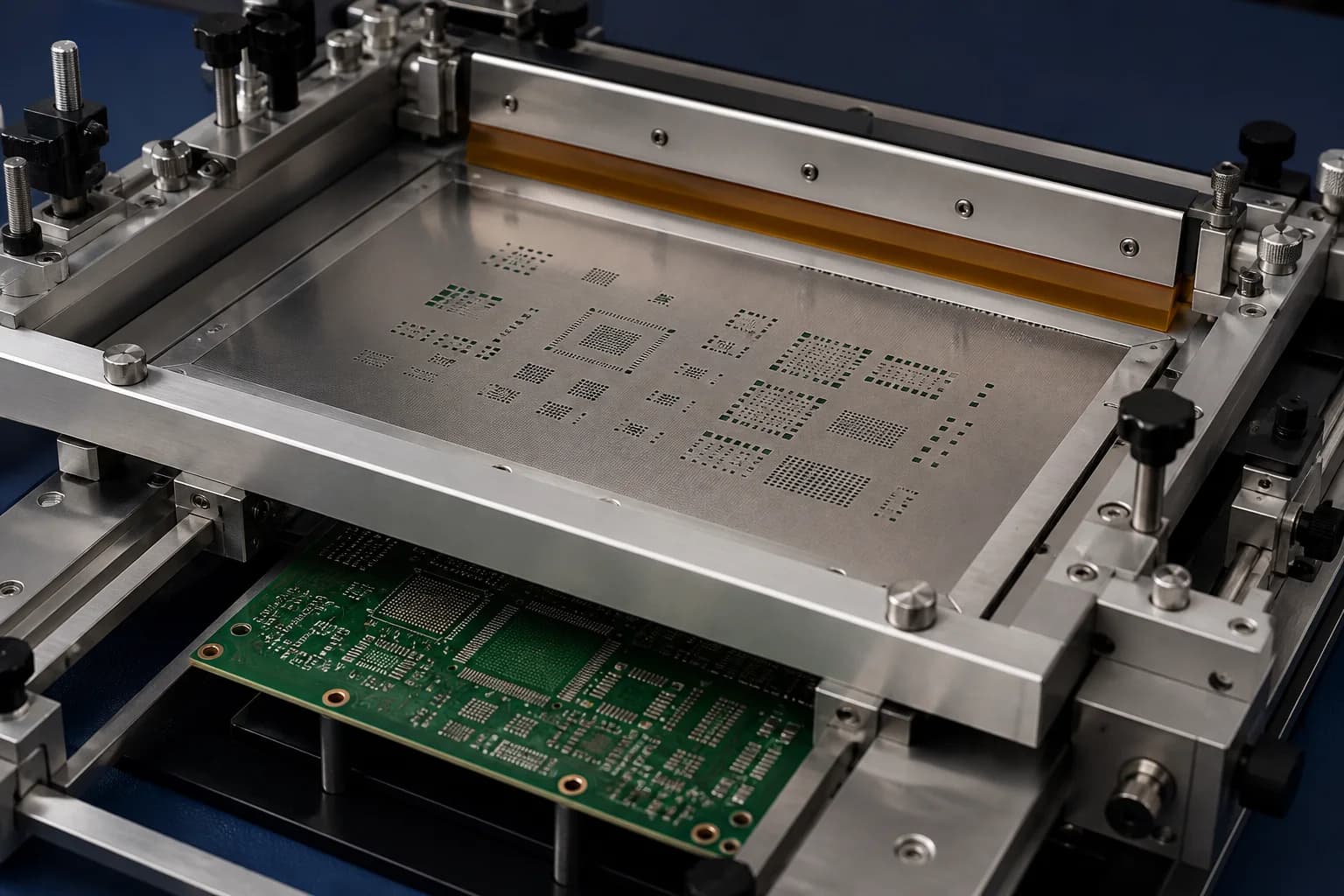
A PCB stencil controls how solder paste is deposited onto the board before component placement. SMT tooling may also include panel support, fiducials, carriers and other setup items needed to hold the board, align the print and run the defined assembly route.
Fine-pitch, thermal pads, mixed package sizes and board support can pull the print process in different directions. The stencil review makes those tradeoffs explicit.
Set aperture dimensions and reductions from pad geometry, component family and solder-joint objective.
Review aspect ratio, area ratio, spacing and paste-release risk for fine-pitch and miniature packages.
Control paste distribution on large exposed pads to reduce void, float and squeeze-out risk.
Use panel, fiducial, carrier and board-support decisions to keep the stencil aligned through the print cycle.
The reference identifies the inputs required for a usable PCB stencil and SMT tooling plan; final dimensions are generated from the released design.
Provide the current Gerber or ODB++, assembly drawing, package data and panel intent so stencil and tooling can be reviewed against the real build.
| Stencil input | Released copper, paste-mask, assembly drawing, package library and revision |
|---|---|
| Aperture design | Pad geometry, reductions, home-plate or segmented strategy and release direction |
| Stencil thickness | Selected from package mix, paste volume, board construction and process window |
| Fine-pitch review | Area ratio, aspect ratio, spacing, paste release and bridging risk assessed by package |
| Thermal-pad review | Paste distribution planned around void, float, squeeze-out and reflow requirements |
| Alignment | Fiducials, tooling holes, panel rails and datum strategy defined for the board and panel |
| Board support | Carrier, support pins or fixture approach selected for flex, thin or uneven boards |
| Setup evidence | Stencil revision, material, inspection and change record linked to the assembly build |
Stencil engineering can manage paste deposition, but it cannot replace a released land pattern, package definition or assembly drawing. The best result comes from reviewing pad geometry, stencil and inspection access together.
Close the print risks before the stencil is fabricated and the first board reaches the line.
Use dedicated stencil and tooling review when package geometry, board handling or paste control can materially change assembly yield.
Control small apertures, paste release, alignment and inspection access around dense packages.
Coordinate thermal pads, hidden joints, board support and AXI or X-ray evidence.
Use carriers and support decisions to stabilize the print and placement route.
Quality documents
The published ISO records name Zhongshan Wenquan Electronic Manufacturing Co., Ltd. and its Zhongshan PCBA facility. They do not certify every PCBArise facility, service or product.


These are management-system certificates, not product or batch COAs. No batch inspection reports or COAs are currently published here.
Use these stencil answers to connect print quality, package geometry, board support and assembly change control.
A PCB stencil deposits solder paste onto the defined board pads before SMT placement. Aperture, thickness and alignment are selected from the package mix and assembly process.
Review pad geometry, aperture reduction, area ratio, aspect ratio, spacing, paste release, support, fiducials and inspection access against the released board and package data.
They can be reviewed together. Panel rails, carriers, support pins, tooling holes and fixtures are included only when the board, panel and assembly route require them.
Yes. Stencil revision, material, aperture changes and the related assembly revision should be recorded so repeat builds use the approved print setup.
Review stencil choices alongside SMT, fine-pitch, BGA, testing and turnkey assembly requirements.
Share the current PCB data, paste-mask, assembly drawing, package mix and panel intent for a stencil and tooling review.