
SMT, THT and mixed
Select the assembly route from package mix, solder access, thermal mass and board support.
PCB Assembly Capabilities covers SMT, THT/DIP, BGA, QFN, fine-pitch and mixed-technology assembly, together with the published PCBA process envelope, inspection methods, testing options and standard lead times for engineering review.

PCB assembly capabilities describe the process, equipment fit and acceptance evidence available for a specific build. The review connects board format, package families, SMT or THT sequence, soldering, inspection, programming and electrical testing instead of treating a machine list as a blanket promise.
The PCBA capability decision connects assembly technology, package geometry, board format, value-added services and acceptance evidence.
Select the assembly route from package mix, solder access, thermal mass and board support.
Review land pattern, stencil, placement, inspection access and rework risk together.
Confirm handling, carriers, panelization and thermal profile for the selected board construction.
Define BOM review, alternates, programming, coating, cable, packaging and delivery requirements.
These published values define the PCBA screening envelope. Maximums and process settings apply to the relevant equipment or assembly line and require confirmation from the released production package.
Use the table for initial supplier review; final equipment, facility, fixture, material and acceptance scope are confirmed before quotation and production release.
| Minimum component size | 01005 (0.4 × 0.2 mm) |
|---|---|
| Component size range | 01005 to 150 × 100 × 30 mm |
| Minimum BGA pitch | 0.25 mm |
| Minimum QFP / QFN pitch | 0.15 mm spacing / 0.3 mm width |
| Placement accuracy (X/Y) | ±0.025 mm (±25 μm) |
| Placement accuracy (θ) | ±0.2° |
| Maximum BGA component size | 70 × 74 mm |
| Maximum PCB assembly size | 400 × 1200 mm; minimum 50 × 50 mm. Applicable process-line envelope; board support and panelization require engineering review. |
| PCB thickness range | 0.3–10.0 mm |
| Warpage control | ≤0.5%; subject to board construction and assembly process review |
| Maximum component height | 120 mm; applicable equipment and assembly route, subject to package-clearance review |
| Soldering methods | Wave soldering; selective soldering; hand soldering |
| Reflow atmosphere | Air / nitrogen. Nitrogen reflow and oxygen targets depend on the assigned line, paste, components and profile. |
| SMT production capacity | 700+ million component placements / month across 20+ SMT lines; combined network figure, not a per-facility or per-line guarantee |
Technologies, substrates and value-added operations
| Assembly technologies | SMT Assembly; THT / DIP Assembly; BGA Assembly; QFN Assembly; Fine-Pitch Assembly; Mixed-Technology Assembly |
|---|---|
| Advanced package and connection types | PoP; Press-Fit; Odd-Form Components |
| Supported substrates | Rigid PCB; Metal-Core PCB; FPC; Rigid-Flex PCB |
| Value-added services | Component Sourcing; BOM Review; Alternative Components; IC Programming; Conformal Coating; Cable & Harness Assembly; Box Build; Final Packaging; Global Delivery |
Process, electrical, functional and traceability evidence
| 3D AOI | False positive rate ≤0.1%; inspection coverage and acceptance scope are confirmed per build |
|---|---|
| 3D SPI | Printing accuracy ±25 μm; result depends on stencil, paste and package mix |
| 2D / 3D AXI | BGA void detection ratio <10%; hidden-joint coverage depends on package and imaging plan |
| ICT | Bed-of-nails / flying probe; 100% netlist check where fixture and access support it |
| FCT | Custom test fixture and application-level validation from the approved procedure and limits |
| Burn-In / aging test | Optional 24 / 48 / 72 hours, subject to product requirements and test plan |
| Boundary Scan / JTAG | Available for complex digital circuits when the device chain and procedure are defined |
| MES traceability | Component-level to panel-level records according to the agreed sourcing and documentation scope |
Business-day planning ranges after file and material review
| Prototype assembly | Standard: 3–5 business days; rush option: 24–48 hours, subject to files, materials and line availability |
|---|---|
| Small-batch / low-volume assembly | Standard: 5–7 business days; expedited option: 3–4 days, subject to BOM and setup requirements |
| Mass production | Standard: 10–15 business days; final schedule depends on BOM availability, demand plan and production allocation |
Response target and schedule conditions
| PCB quotation response | Target within 24 hours after a complete Gerber package is received; engineering review and final quotation depend on file completeness and project scope |
|---|---|
| PCBA quotation response | Target within 24 hours after the required Gerber, BOM, CPL and assembly information is received; schedule depends on material and test requirements |
| Lead-time basis | All lead times are business-day planning ranges subject to production files, process complexity, BOM availability, fixtures and line scheduling |
For a complete Gerber package, PCBArise targets a quotation and engineering-review response within 24 hours. PCBA timing is confirmed only after the BOM, CPL, board format, process route, material availability, fixtures and test requirements are reviewed.
The final route connects the design files to the equipment, materials and acceptance evidence for that build.
Choose the page that answers the next engineering or purchasing decision.
Review 01005, BGA, QFN, stencil, placement and reflow constraints.
Review wave, selective, hand-soldering, odd-form and press-fit requirements.
Define SPI, AOI, AXI, ICT, FCT, programming and MES evidence.
Use the lead-time ranges after BOM, fixture and process readiness are confirmed.
Quality documents
The published ISO records name Zhongshan Wenquan Electronic Manufacturing Co., Ltd. and its Zhongshan PCBA facility. They do not certify every PCBArise facility, service or product.
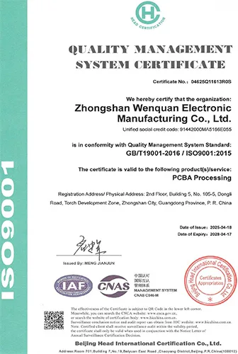
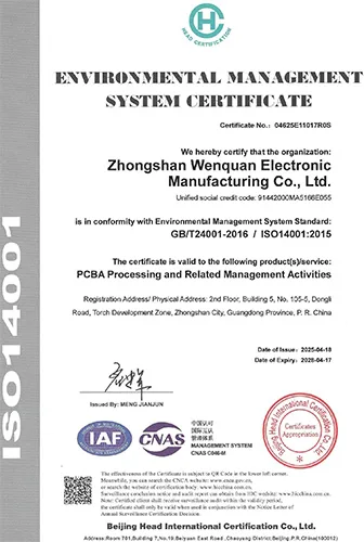
These are management-system certificates, not product or batch COAs. No batch inspection reports or COAs are currently published here.
Use these capability answers to prepare a supplier-qualification package and separate confirmed process fit from assumptions.
The published scope includes SMT, THT/DIP, BGA, QFN, fine-pitch and mixed-technology assembly, together with PoP, press-fit and odd-form components. Final fit depends on the released board and package data.
The reference range is 01005 components, 0.25 mm minimum BGA pitch, ±0.025 mm X/Y placement accuracy, 0.3–10.0 mm PCB thickness and a 50 × 50 mm to 400 × 1200 mm assembly envelope for applicable process lines.
The number is a published process-envelope reference, not a blanket claim for every facility. Board support, panelization, equipment, clearance and line assignment are confirmed during engineering review.
The reference includes 3D SPI, 3D AOI, 2D/3D AXI, ICT, flying probe, FCT, optional burn-in, Boundary Scan/JTAG and MES traceability. The final plan is selected by product risk and test access.
Prototype assembly is planned at 3–5 business days, small-batch assembly at 5–7 business days and mass production at 10–15 business days, with expedited options subject to BOM, fixtures, process readiness and line scheduling.
These value-added operations can be evaluated when the approved firmware, drawings, coating requirements, cable or harness data, packaging and acceptance criteria are available.
Connect the process envelope to SMT, turnkey, prototype and component-sourcing pages without leaving the existing Assembly menu.
Send the released board, assembly, BOM, CPL and test information. Complete files receive a quotation and engineering-review response target within 24 hours, subject to scope.