
Single-sided
Copper on one side for simple power, LED and low-density control boards.
Rigid PCB manufacturing provides a stable platform for fixed mechanical assemblies, from single-sided circuits to controlled-impedance multilayer boards.
Rigid PCB is not one process window. Layer count, copper weight, laminate and via structure change cost and production risk in different ways.
Copper on one side for simple power, LED and low-density control boards.
Plated through-holes and routing on both sides—the standard entry point for prototypes.
Internal planes, impedance references and additional routing channels for complex electronics.
Heavy copper, metal-core and high-frequency materials require their own stackup decisions.
Designs inside the standard window quote faster and carry lower process risk. Advanced combinations still require file-level evaluation.
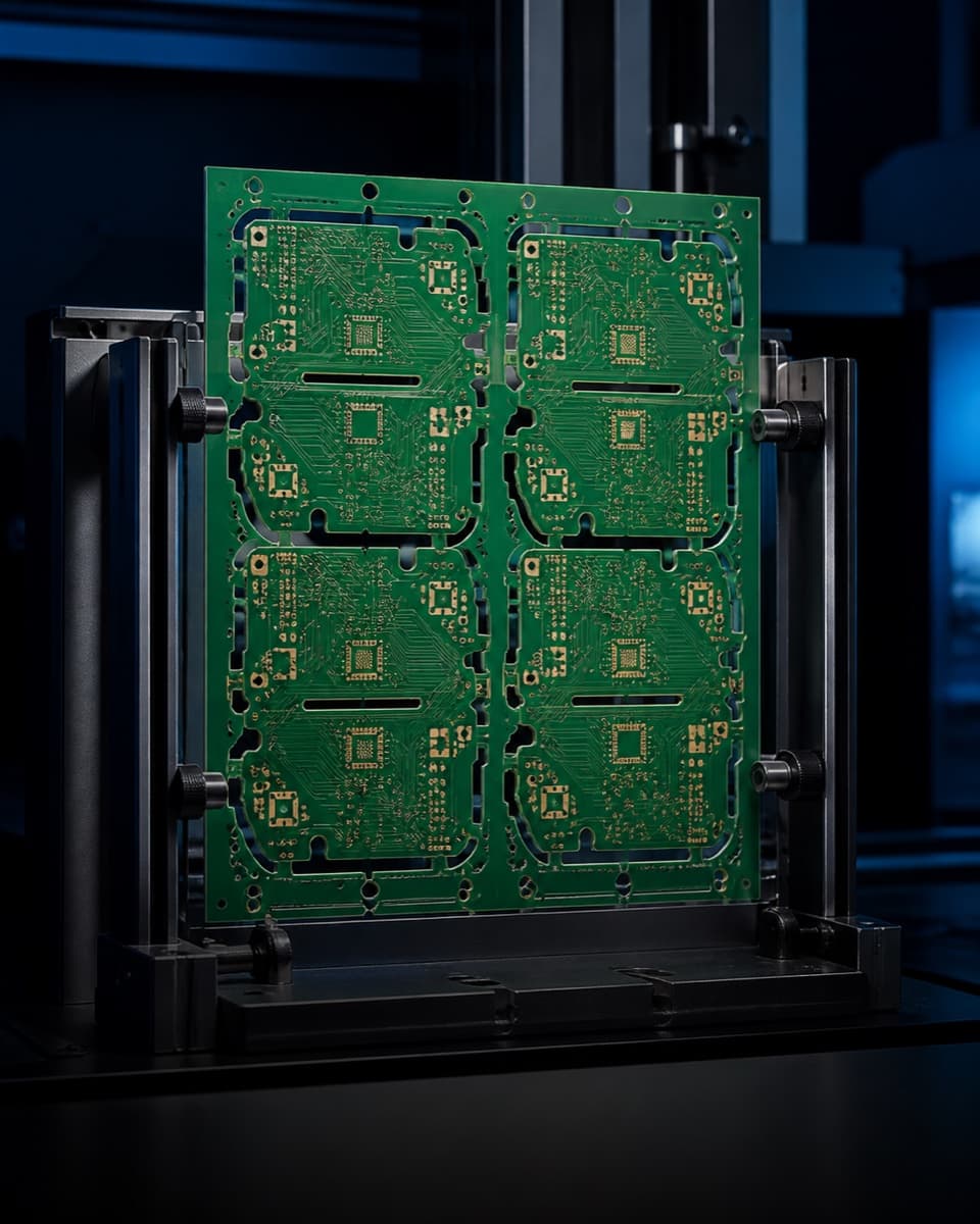
Volume production capability for standard builds
| Layer count | 1–40 layers |
|---|---|
| Base materials | FR-4, High-Tg FR-4, halogen-free FR-4, Rogers, Taconic/AGC, PI, aluminum, PTFE/Teflon, F4B and other specialty laminates |
| Board thickness | 0.10–10.0 mm |
| Minimum trace / spacing | 2.5 / 2.5 mil (0.0625 / 0.0625 mm) |
| Minimum mechanical drill | 0.15 mm |
| Minimum laser via | 0.10 mm |
| Standard aspect ratio | Up to 15:1 |
| Copper thickness | 0.5–12 oz, depending on board type and construction |
| Controlled impedance | ±10% standard; ±5% for tighter requirements |
| Warpage | ≤0.75% standard; ≤0.5% available when specified |
| Surface finishes | HASL, Lead-Free HASL, OSP, ENIG, Immersion Silver, Immersion Tin, ENEPIG, Hard Gold, Gold Finger and selective finishes |
Capability values are design-dependent. Material, copper weight, layer count, via structure, finished thickness and surface finish can change the achievable combination.
FR-4 is the default. High-Tg TG170 is appropriate for repeated lead-free reflow or elevated operating temperatures. Controlled-Dk laminates should be confirmed before layout is frozen.
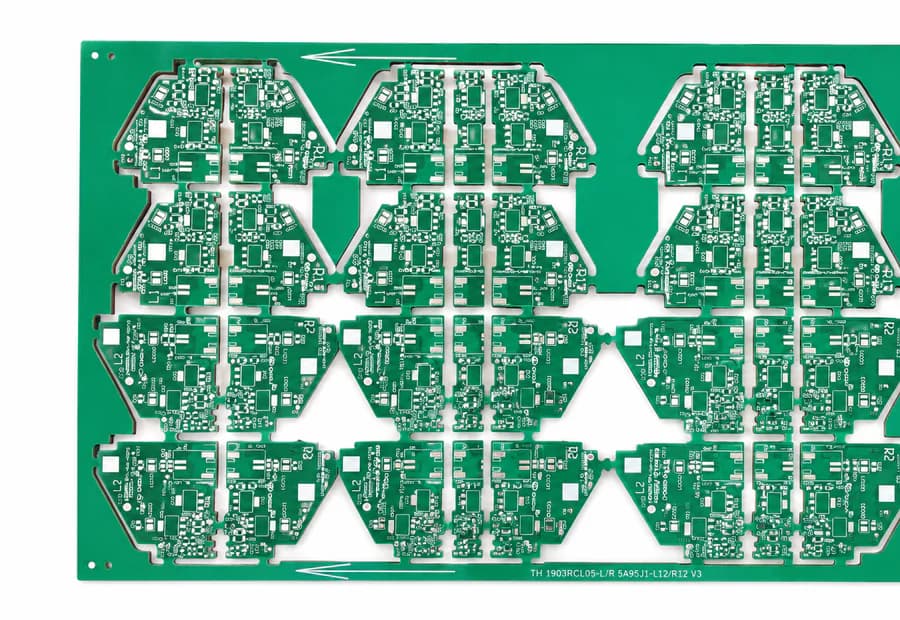
Check copper weight, drill geometry, annular ring, stackup balance and target impedance against the selected rigid PCB process.
Use these examples as a starting point. The board construction still follows the product’s electrical, mechanical and qualification requirements.
Fixed-geometry control, instrumentation and motor-drive electronics.
Power supplies and DC-DC conversion, including heavier copper requirements.
Control units and supporting electronics built to the specified acceptance criteria.
Rigid or metal-backed boards selected around the required thermal path.
Appliances and commercial devices with stable mechanical packaging.
Networking cards and backplanes where stackup and impedance matter.
Quality documents
The published ISO records name Zhongshan Wenquan Electronic Manufacturing Co., Ltd. and its Zhongshan PCBA facility. They do not certify every PCBArise facility, service or product.
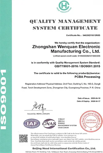
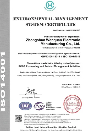
These are management-system certificates, not product or batch COAs. No batch inspection reports or COAs are currently published here.
Use these answers to prepare a rigid PCB package for quotation and manufacturing review.
Volume production supports 1–40 layers. Prototype and engineering builds can support up to 64 layers; the complete stackup determines feasibility.
The standard process window is 2.5/2.5 mil. Advanced 2/2 mil geometries are evaluated against copper weight, laminate and the rest of the stackup.
Standard controlled impedance is ±10%. ±5% is available for tighter requirements when the laminate, stackup and thickness control support it.
ENIG is commonly selected for fine-pitch and BGA assembly. OSP and HASL can be appropriate for cost-led designs, while ENEPIG supports specific bonding and shelf-life requirements.
Move from rigid FR-4 to denser stackups, fabrication limits, DFM review or prototype validation.
Share the available Gerber, ODB++, drawing, stackup or project requirements with the PCBArise team.