
Gerber and drill
Trace, spacing, annular ring, drill-to-copper, board outline and solder-mask checks.
Before tooling starts, a PCB DFM review checks whether the board you designed can be built and assembled as intended. PCBArise looks for file mismatches, stackup, drill, copper, spacing and assembly-access issues that are easier to fix now than on the production line.
For stackup, layout checks and release files, use the PCB design guide.
A useful DFM review does more than run generic rules. It connects the design package to material, drilling, imaging, lamination and assembly process limits.
Trace, spacing, annular ring, drill-to-copper, board outline and solder-mask checks.
Layer order, dielectric thickness, copper balance, reference planes and target impedance.
Footprints, package availability, fine-pitch geometry, panel fiducials and paste-aperture risk.
Electrical test, inspection access, test-point coverage and custom acceptance needs.
These values establish the standard screening window. Advanced and flexible designs are checked against their own qualified processes.

Baseline checks for rigid and multilayer PCB
| Layer count | 1–40 layers |
|---|---|
| Base materials | FR-4, High-Tg FR-4, halogen-free FR-4, Rogers, Taconic/AGC, PI, aluminum, PTFE/Teflon, F4B and other specialty laminates |
| Board thickness | 0.10–10.0 mm |
| Minimum trace / spacing | 2.5 / 2.5 mil (0.0625 / 0.0625 mm) |
| Minimum mechanical drill | 0.15 mm |
| Minimum laser via | 0.10 mm |
| Standard aspect ratio | Up to 15:1 |
| Copper thickness | 0.5–12 oz, depending on board type and construction |
| Controlled impedance | ±10% standard; ±5% for tighter requirements |
| Warpage | ≤0.75% standard; ≤0.5% available when specified |
| Surface finishes | HASL, Lead-Free HASL, OSP, ENIG, Immersion Silver, Immersion Tin, ENEPIG, Hard Gold, Gold Finger and selective finishes |
Inputs reviewed before the fabrication package is released to PCBA
| Package and footprint fit | Component body, land pattern, polarity, height and inspection access reviewed against the released package |
|---|---|
| Board and panel format | Board outline, tooling rails, fiducials, support and panelization reviewed for the intended assembly route |
| Assembly process access | SMT / THT sequence, solder access, clearance, thermal exposure and rework boundary reviewed together |
| Test access | Test points, probe access, programming interface and functional-test requirements defined before release |
Capability values are design-dependent. Material, copper weight, layer count, via structure, finished thickness and surface finish can change the achievable combination.
Critical findings are separated from advisory improvements. Production starts from the approved file package, after questions are resolved and revisions are aligned.

Separate release-blocking findings from advisory improvements, resolve open questions and confirm one approved production package.
Use these examples as a starting point. The board construction still follows the product’s electrical, mechanical and qualification requirements.
Gerber RS-274X or ODB++, NC drill and board outline.
Finished thickness, copper, finish, tolerance and IPC class.
Material, layer order and controlled-impedance targets.
BOM, pick-and-place and assembly drawings when PCBA is included.
Electrical, ICT, flying-probe, functional or custom verification.
A single approved data package with matching revision identifiers.
Quality documents
The published ISO records name Zhongshan Wenquan Electronic Manufacturing Co., Ltd. and its Zhongshan PCBA facility. They do not certify every PCBArise facility, service or product.
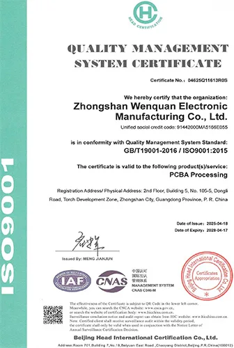

These are management-system certificates, not product or batch COAs. No batch inspection reports or COAs are currently published here.
These answers cover review scope, required files, revision control and the handling of manufacturing findings.
The existing service model includes DFM review with the quotation and active order evaluation. The design package is reviewed before production release.
Send Gerber RS-274X or ODB++, NC drill, fabrication drawing and stackup. Add BOM, pick-and-place and assembly drawings when assembly is included.
Findings and proposed corrections are returned for approval. The production package remains under customer revision control and is only released after alignment.
Common findings include insufficient annular ring, drill-to-copper clearance, copper imbalance, unsuitable via structures, incomplete fabrication notes and BOM-to-footprint mismatch.
Use the approved data package to confirm capability, board construction and the prototype or production route.
Share the available Gerber, ODB++, drawing, stackup or project requirements with the PCBArise team.