
PCBArise / Articles
PCB Manufacturing and Assembly Guides
Use these practical articles to qualify suppliers, compare assembly routes, plan inspection and make a clearer PCB or PCBA sourcing decision.
Latest
Start with the decision closest to your project.
Each article turns a common procurement or engineering question into a practical checklist.
 AI-generated illustration
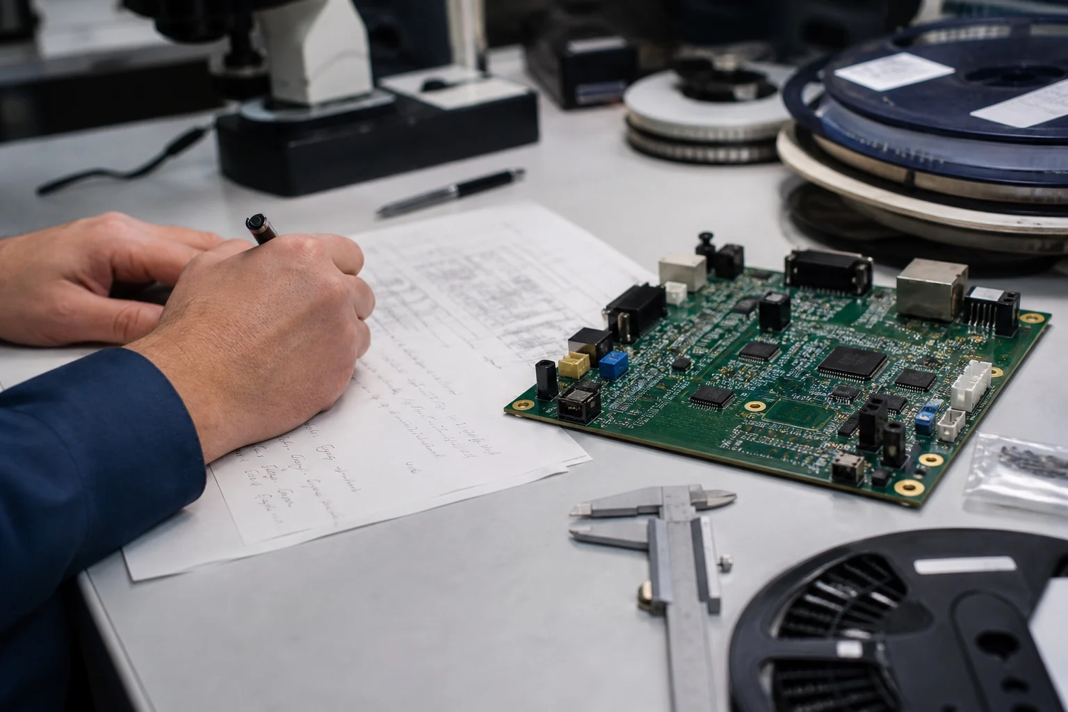
Reels, Trays, Tubes and Cut Tape: Preparing SMT Materials
Prepare reels, trays, tubes and cut tape for SMT with identity, count, orientation, feeder-readiness and discrepancy records that prevent avoidable line-side surprises.
Read article →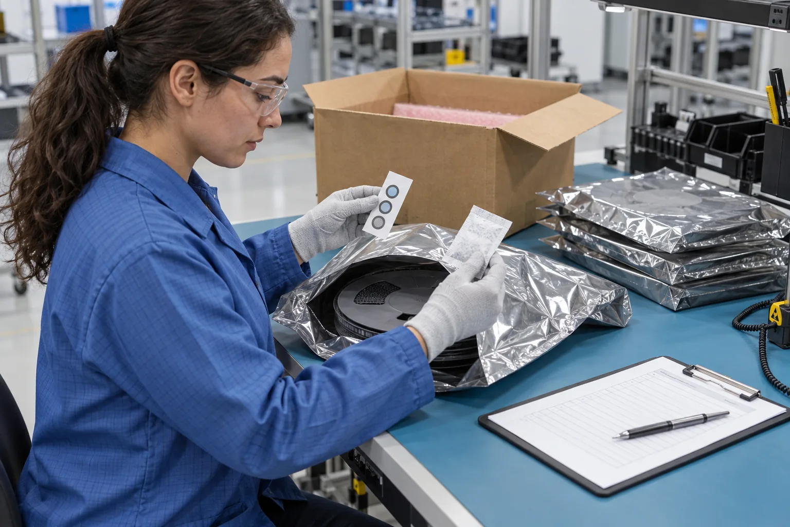 AI-generated illustration
Moisture-Sensitive Components: Handling Before PCB Assembly
Prepare moisture-sensitive components for PCB assembly with receiving checks, cumulative exposure records, hold decisions and a copyable MSL handoff log.
Read article → AI-generated illustration
PCBA Rework and Repair: Acceptance Criteria That Must Be Defined
Define PCBA rework acceptance criteria for components, pads, traces, holes, solder mask, cleanliness, heat exposure, records and post-rework inspection and test.
Read article →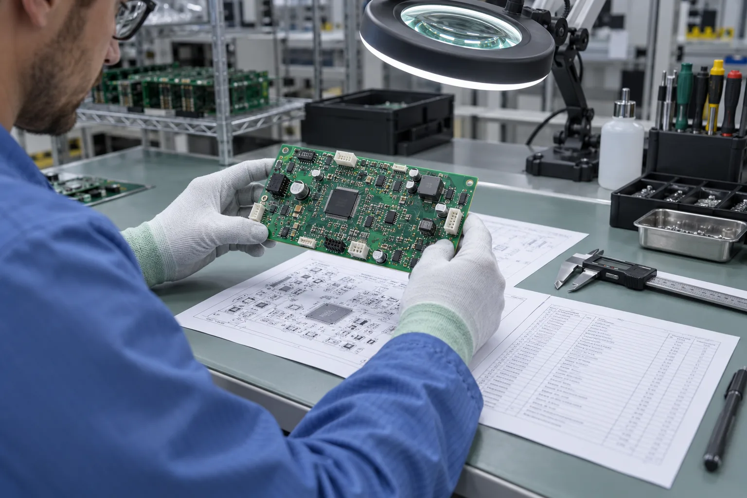 AI-generated illustration
First-Article Inspection for PCBA Pilot Builds
Use a practical PCBA first article inspection checklist to verify released files, materials, placement, soldering, firmware, function and open issues before a pilot lot continues.
Read article →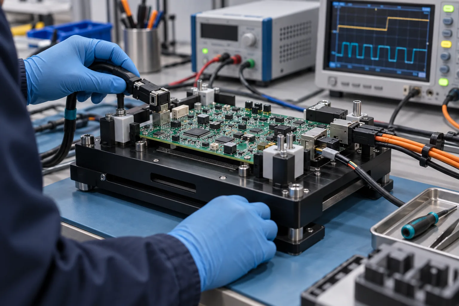 AI-generated illustration
Functional-Test Fixture Brief for a PCBA Pilot Build
Write a functional-test fixture brief for a PCBA pilot build: DUT interfaces, power, loads, firmware, limits, versions and results needed for repeat production.
Read article →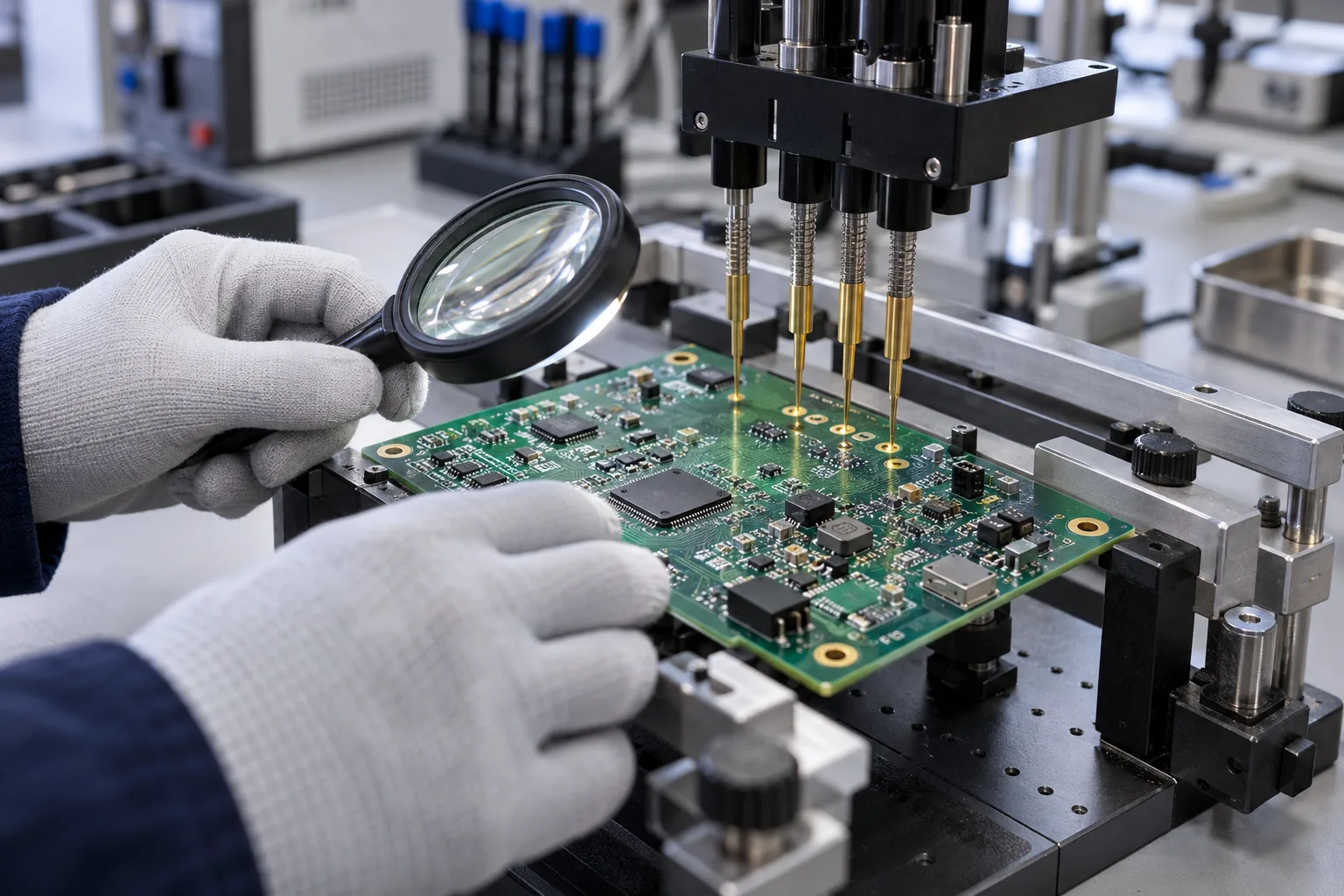 AI-generated illustration
Test-Point Design for ICT and Flying Probe
Design PCB test points that ICT fixtures and flying probes can reach, then document net priority, access, keepouts and board support for the test handoff.
Read article →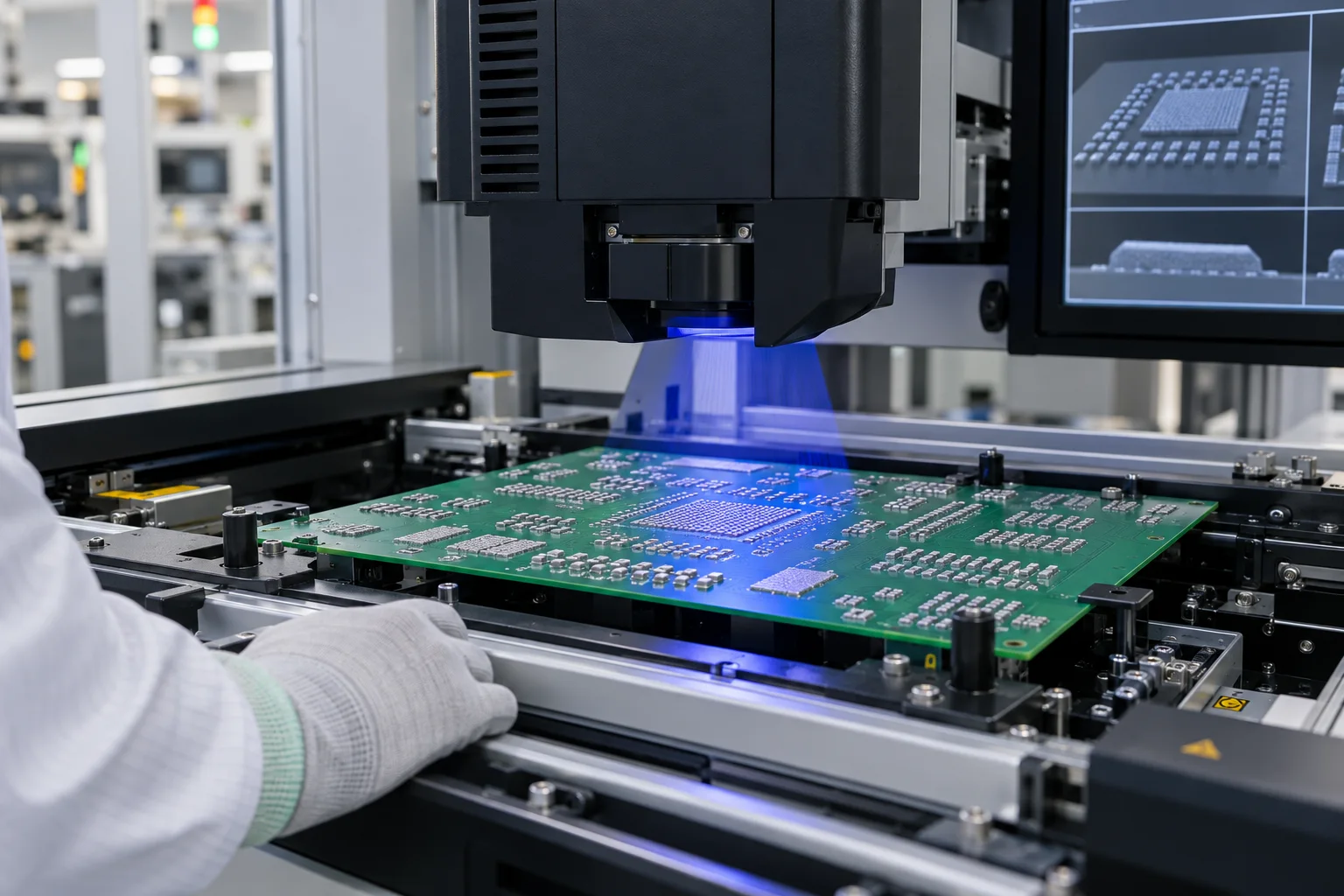 AI-generated illustration
What Solder Paste Inspection Can—and Cannot—Show
See what solder paste inspection SPI measures before placement, what it cannot prove after reflow, and how to combine SPI with AOI, X-ray and electrical test.
Read article →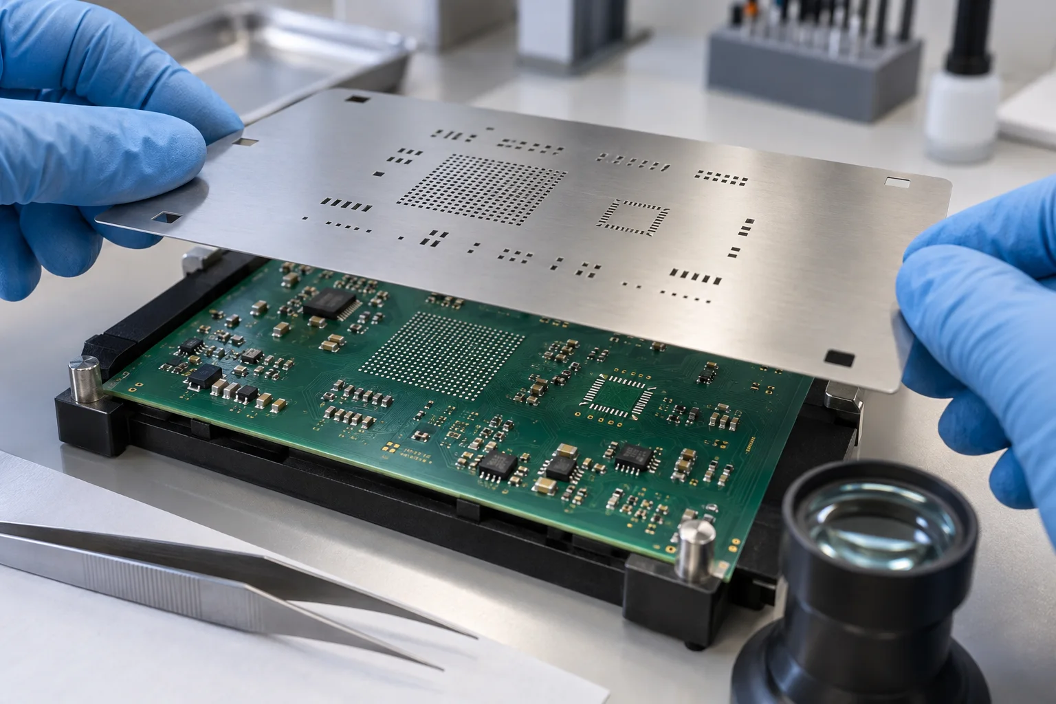 AI-generated illustration
SMT Stencil Apertures: What Changes for BGA and QFN
Design SMT stencil apertures around package land patterns, foil thickness and paste release. Learn why BGA and QFN deposits need different decisions.
Read article →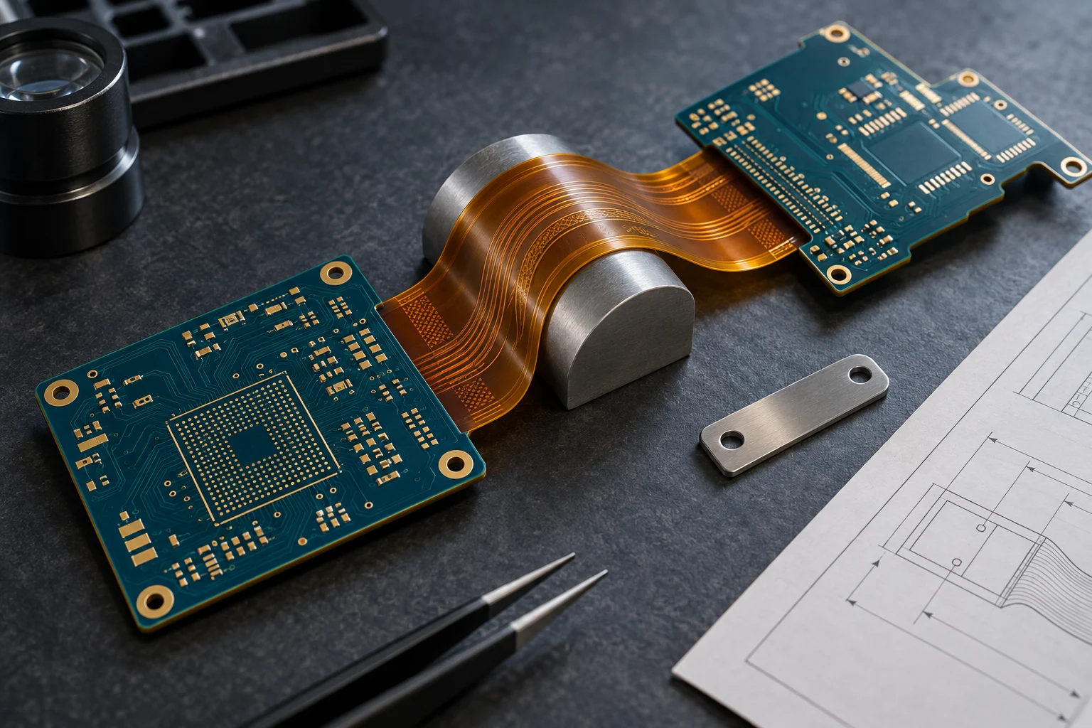 AI-generated illustration
Rigid-Flex Bend Zones: What the Fabricator and Assembler Need
Define rigid-flex bend zones by motion, radius, flex stackup, trace direction, coverlay, stiffeners and assembly support before the board is quoted.
Read article →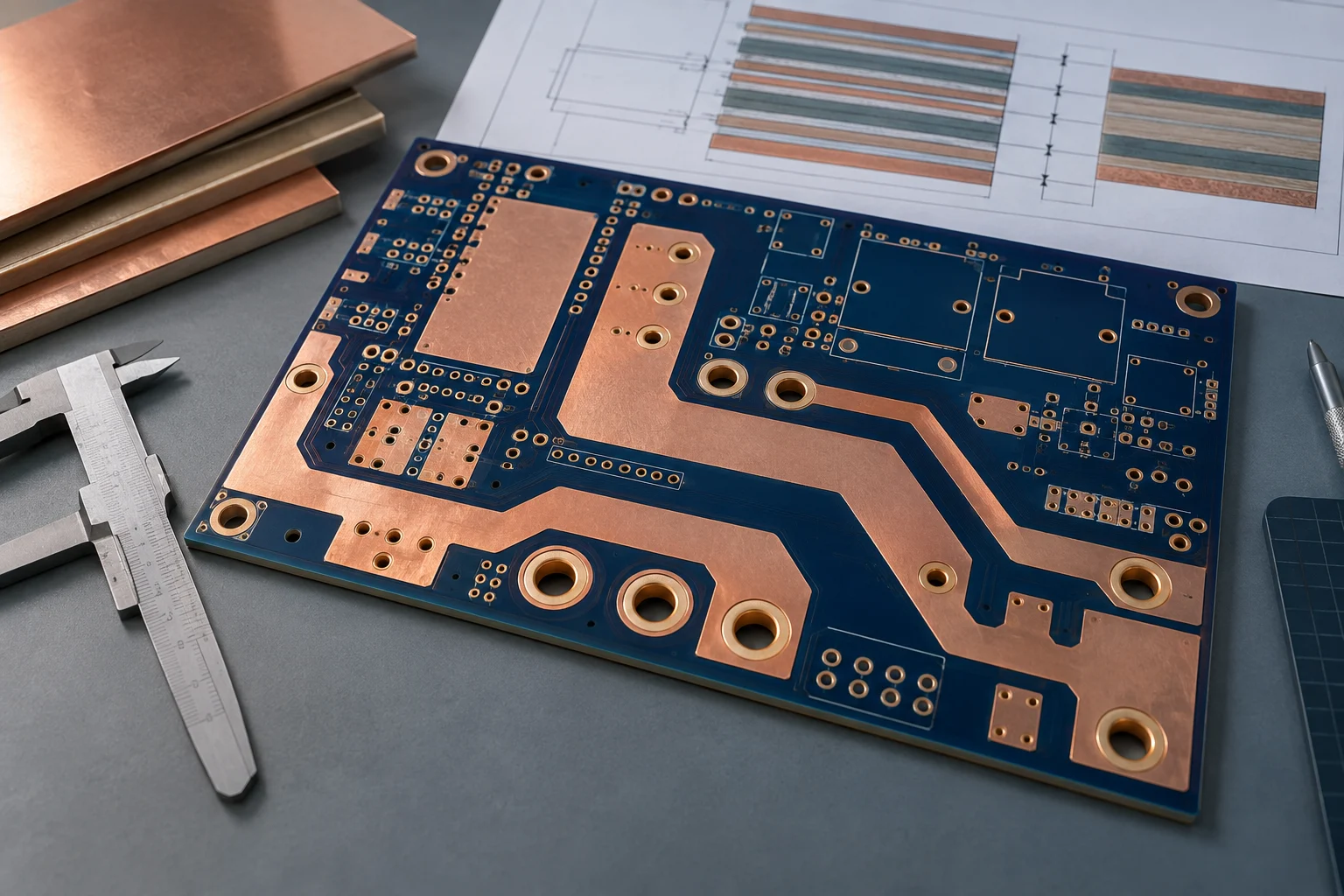 AI-generated illustration
How to Specify Copper Weight for a Power PCB
Specify power-board copper by current path, permitted temperature rise, layer location, finished copper and manufacturability—not by a universal amp rating.
Read article →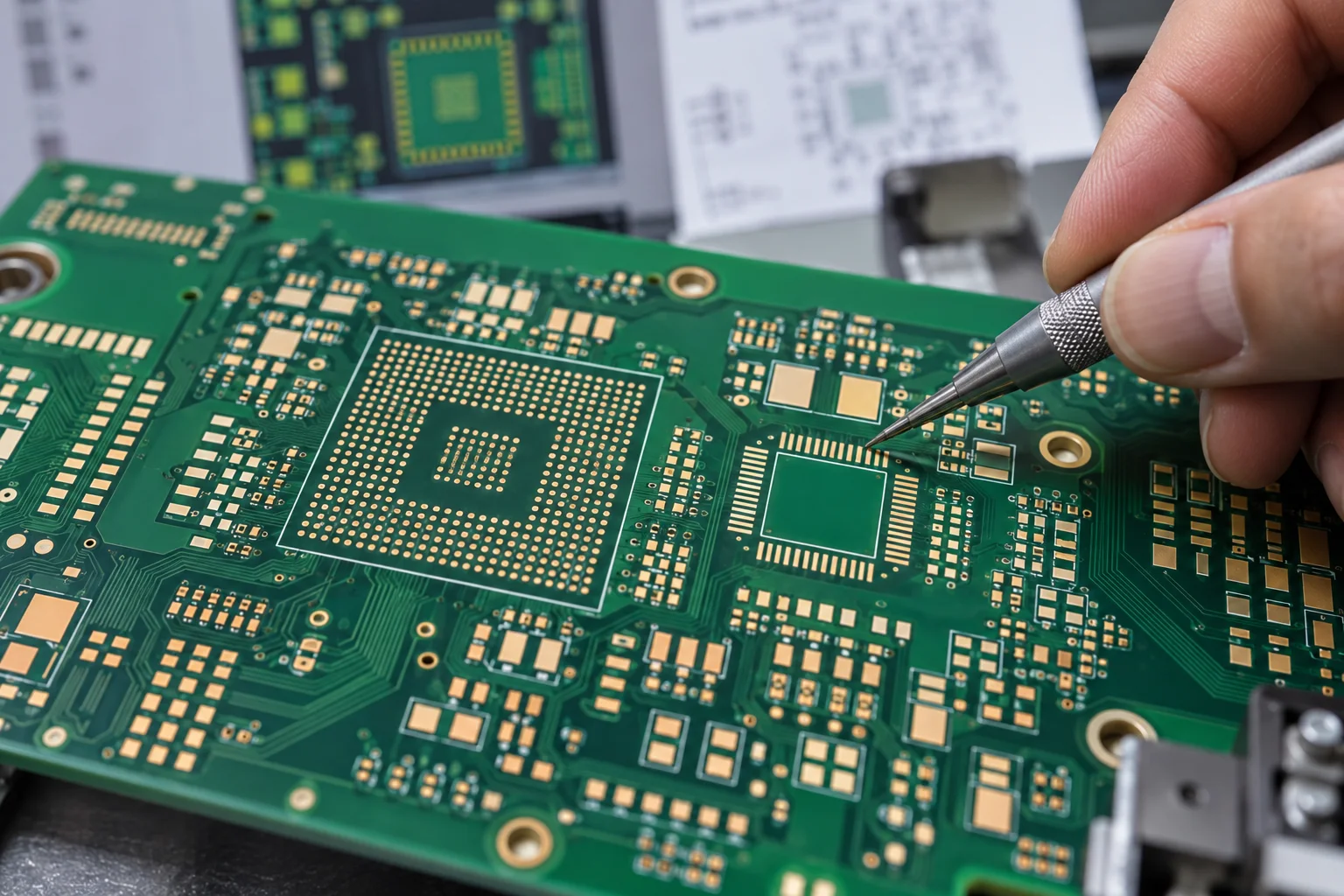 AI-generated illustration
Solder Mask Decisions for Fine-Pitch PCB Assembly
Design fine-pitch solder mask by balancing pad exposure, registration allowance and a stable mask dam—then put the chosen rules in the fabrication data.
Read article →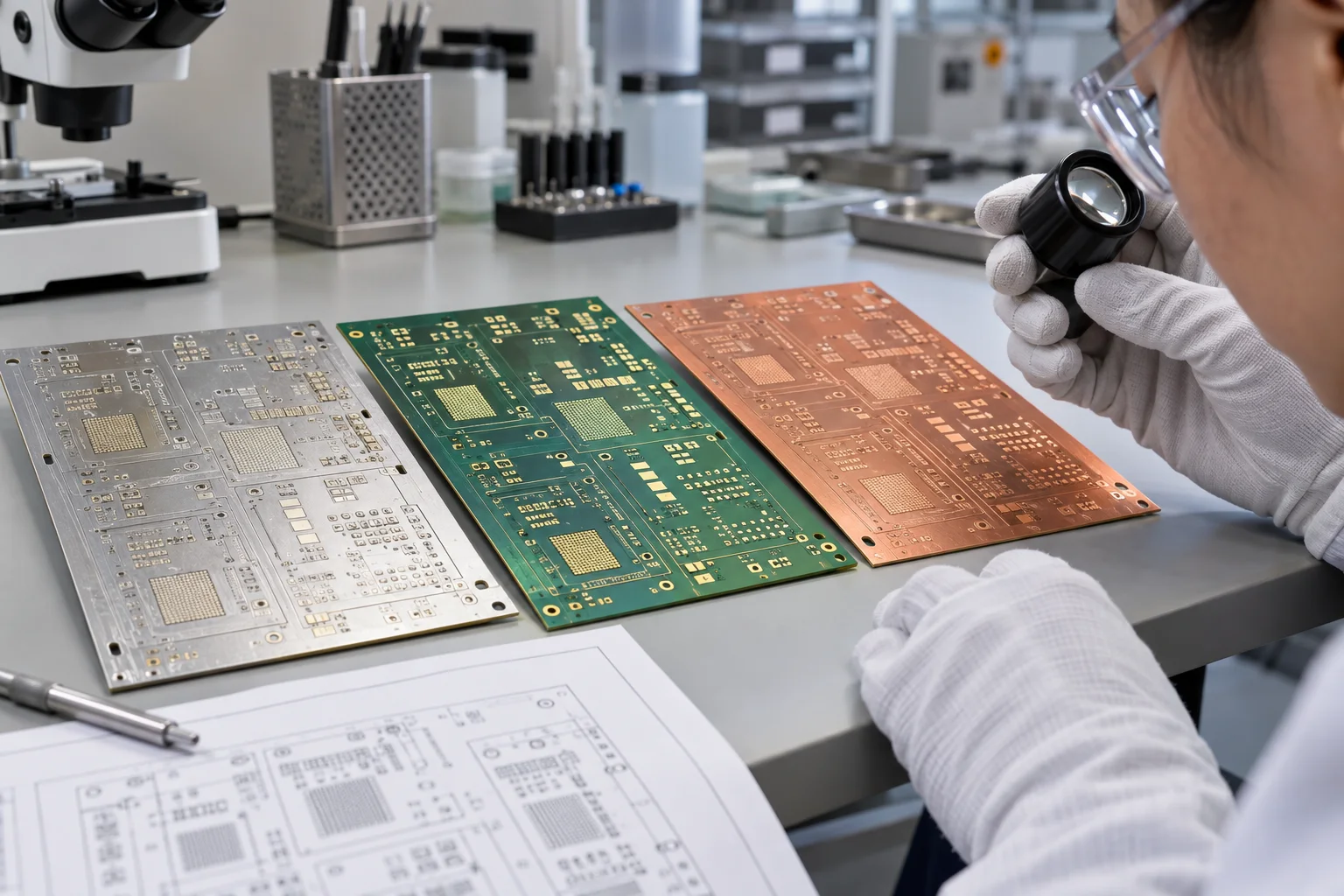 AI-generated illustration
ENIG vs HASL vs OSP: Choosing a PCB Surface Finish
Choose ENIG, lead-free HASL or OSP by pad flatness, assembly route, storage window and cost exposure—not by a one-word “best finish” rule.
Read article →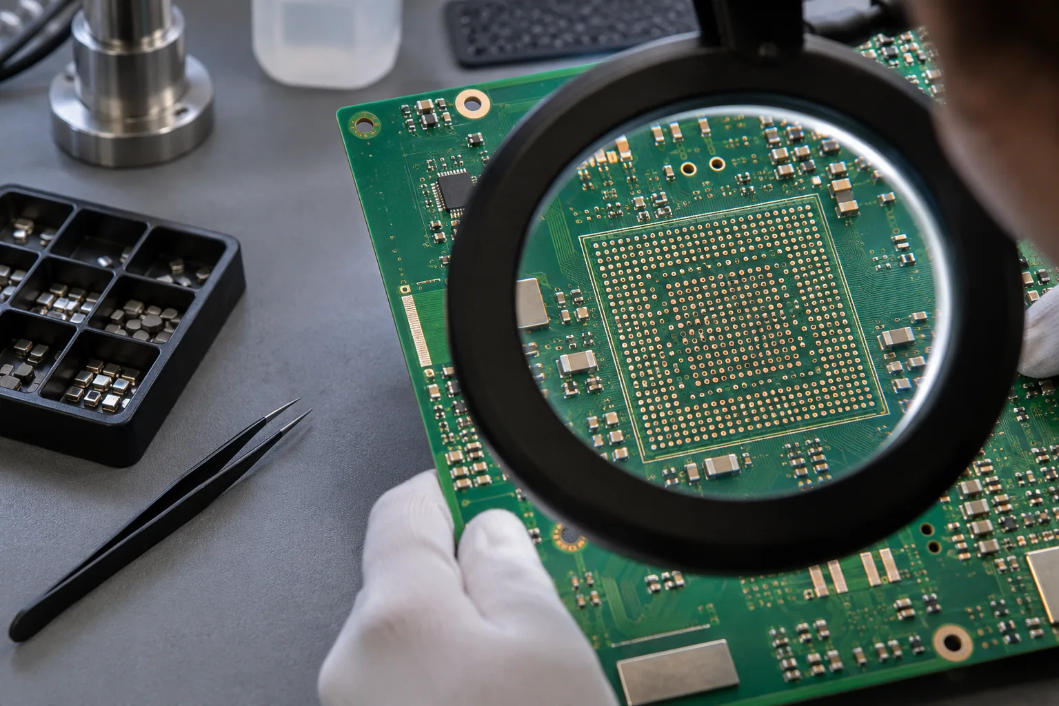 AI-generated illustration
Via-in-Pad vs Microvia: Design and Manufacturing Trade-offs
Via-in-pad describes where a via sits; microvia describes a small HDI via structure. Compare the combinations, BGA escape choices and fabrication notes that prevent solder loss.
Read article →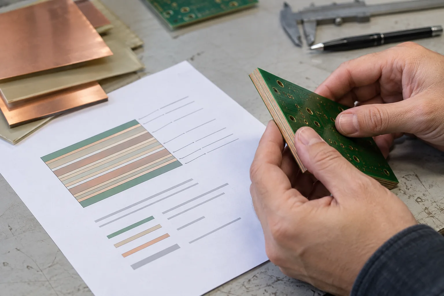 AI-generated illustration
Controlled-Impedance PCB Stackup: What to Specify to a Fabricator
Specify impedance by net class, layer, reference plane, target and tolerance. Use this fabrication-note example and stackup handoff checklist before routing.
Read article →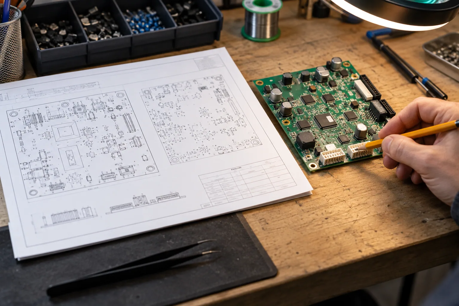 AI-generated illustration
PCB Assembly Drawing Checklist: Polarity, Orientation and Build Notes
Use this PCB assembly drawing checklist to show board views, reference designators, polarity, connector orientation, mechanical details and build exceptions that a BOM or CPL cannot explain.
Read article →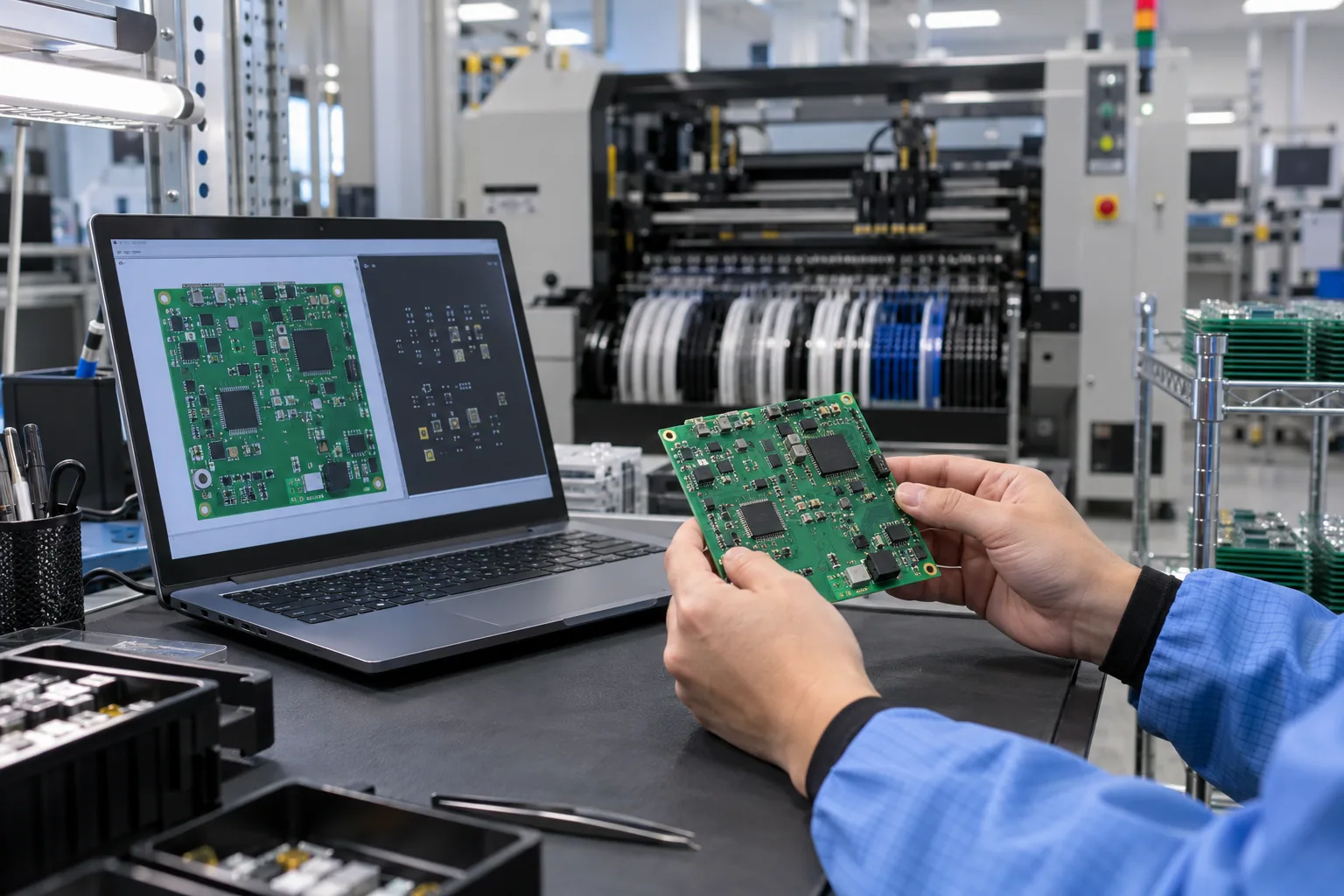 AI-generated illustration
Pick-and-Place File Errors That Delay PCB Assembly
Make your pick-and-place file usable for PCB assembly: check designators, coordinates, origin, side, rotation and BOM alignment before sending the build package.
Read article →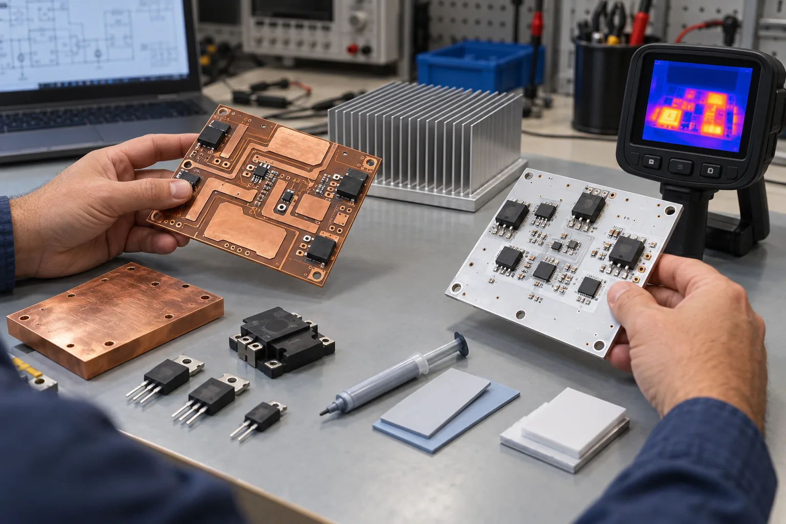 AI-generated illustration
Thermal PCB Design Inputs: Heavy Copper, Metal-Core and Heat Paths
Compare heavy-copper and metal-core PCB designs for current paths, heat spreading, insulation, assembly and thermal verification.
Read article →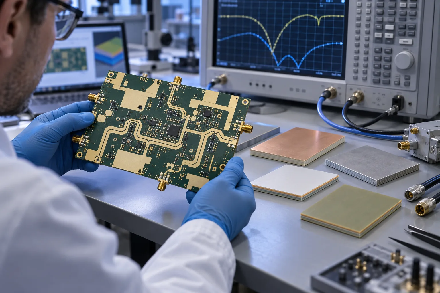 AI-generated illustration
RF PCB Material and Stackup Selection Guide
Choose RF PCB material and stackup around frequency, dielectric data, copper profile, impedance, loss and fabricator tolerances.
Read article →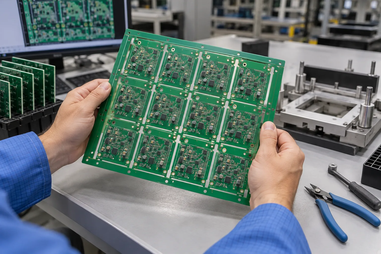 AI-generated illustration
PCB Panelization Guide for Prototype and Production Builds
Plan PCB panelization for prototype and production with rails, tooling holes, fiducials, board spacing, depaneling and assembly handling.
Read article → AI-generated illustration
Low-Volume vs High-Volume PCB Assembly: Route Selection Guide
Compare low-volume and high-volume PCB assembly routes by product maturity, demand, setup, component sourcing and repeatability.
Read article →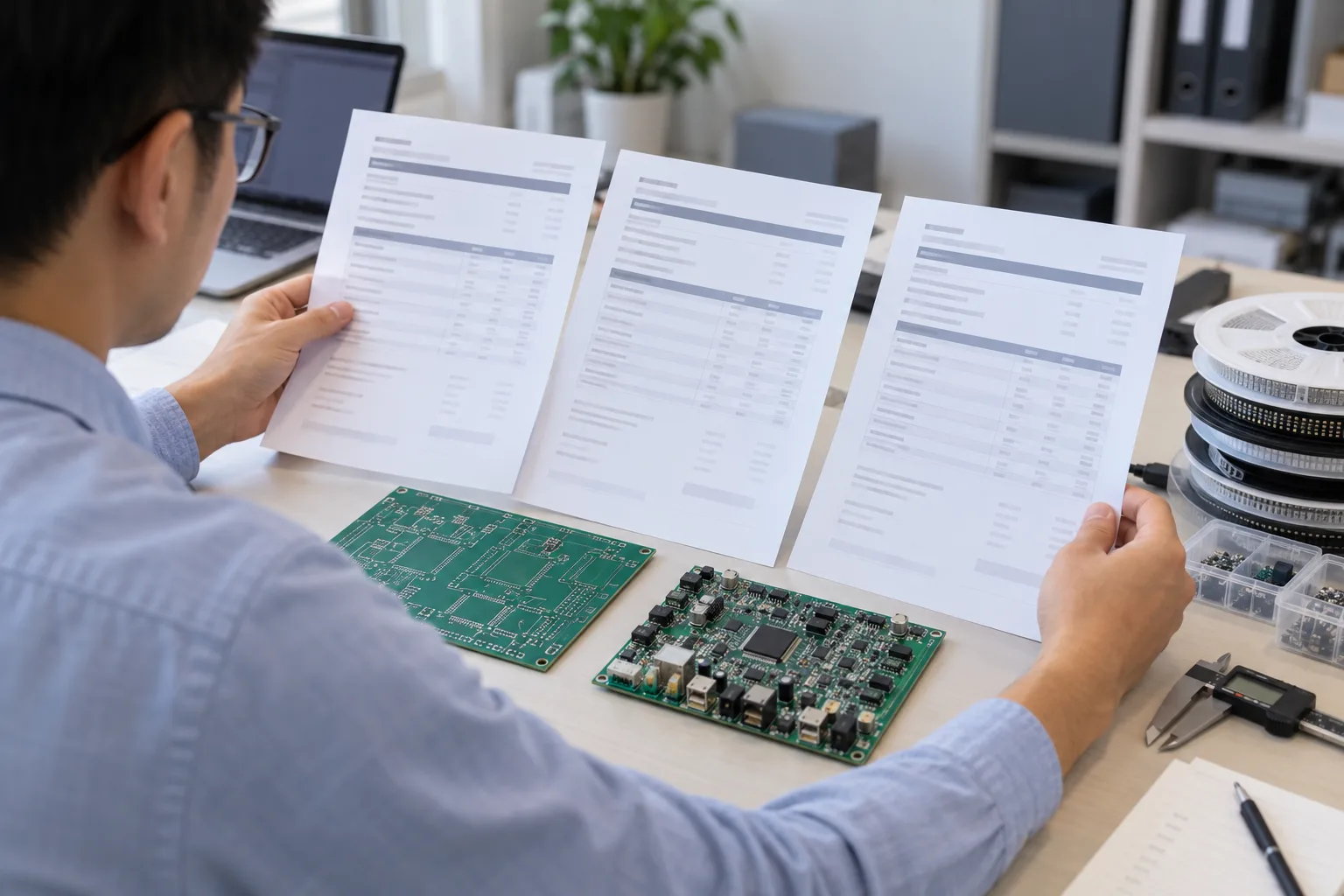 AI-generated illustration
PCB Quote Comparison Checklist: Scope, Testing and Commercial Terms
Compare PCB and PCBA quotes with a checklist for board revision, fabrication, components, assembly, testing, tooling and delivery terms.
Read article → AI-generated illustration
How to Qualify a PCB Manufacturer in China: A Practical Buyer Checklist
Use a practical checklist to choose a PCB manufacturer in China by design fit, fabrication process, quality system, sample build and communication.
Read article →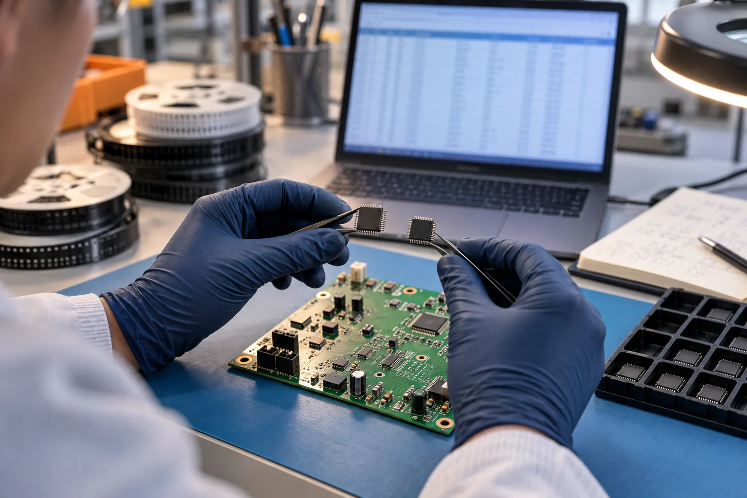 AI-generated illustration
PCB Component Alternates: How to Evaluate a BOM Substitute
Evaluate a PCB assembly component alternate by exact part number, package, pinout, electrical behavior and BOM update before use.
Read article → AI-generated illustration
PCB Assembly Traceability: Lot, Revision and Process Tracking
Understand PCB assembly traceability from board revision and component lots to build identifiers, process checks and test history.
Read article →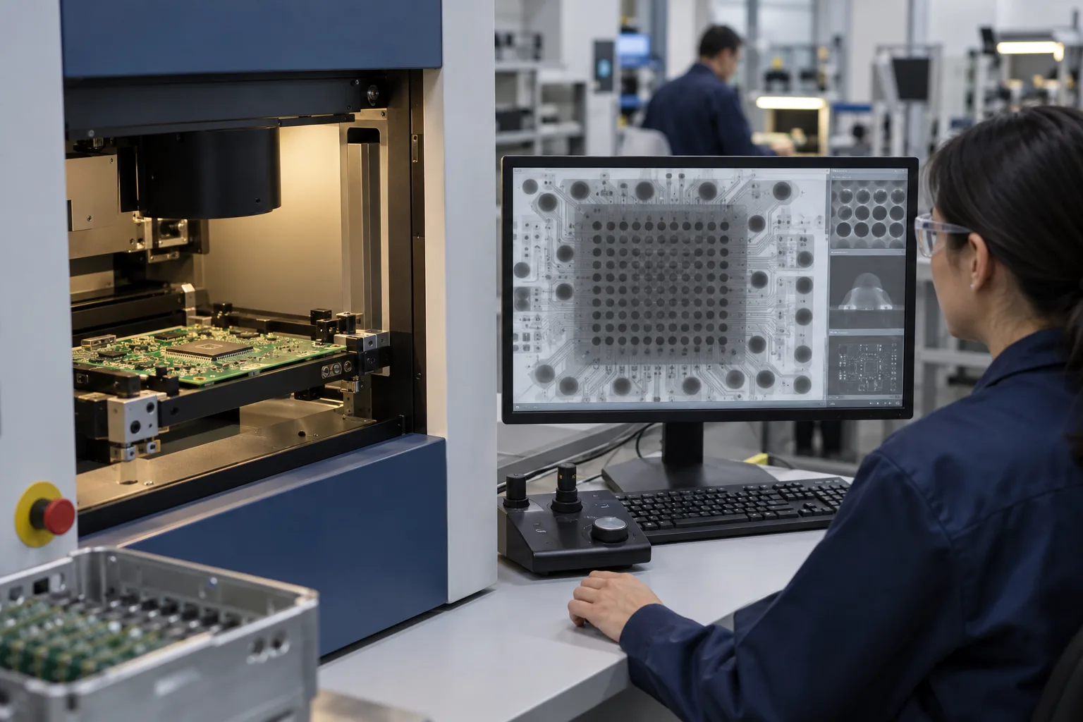 AI-generated illustration
BGA X-Ray Inspection Guide: What It Shows and When to Use It
See when BGA X-ray inspection helps examine hidden solder joints, what a radiograph can show and how it complements AOI and electrical testing.
Read article →
Mixed-Technology PCBA: Planning SMT and THT in One Build
Plan mixed-technology PCBA with both SMT and through-hole parts, including sequence, solder method, tooling, inspection and test.
Read article →
Through-Hole PCB Assembly Design Checklist
Review through-hole PCB assembly design for lead-to-hole fit, mechanical support, soldering access, component clearance and inspection.
Read article →
BOM Preparation for Turnkey PCB Assembly
Prepare a turnkey PCB assembly BOM with exact manufacturer part numbers, reference designators, quantities, DNP lines and approved alternatives.
Read article →
Functional Test vs ICT vs Flying Probe for PCB Assembly
Compare PCBA functional test, ICT and flying probe by what they check, required access, fixture effort and fit for prototype or repeat builds.
Read article →
Prototype to Production PCB Transfer Checklist
Move a PCB prototype to production with a checklist for DFM changes, released files, BOM, sourcing, assembly, test and pilot feedback.
Read article →
PCB Cost Drivers: How to Compare Manufacturing Quotes
Learn the main PCB cost drivers and compare manufacturing quotes across materials, layer count, drilling, finish, assembly, testing and tooling.
Read article →
Gerber vs ODB++ vs IPC-2581: PCB Manufacturing File Guide
Compare Gerber, ODB++ and IPC-2581 for PCB manufacturing data, including package structure, fabrication use and files to include for assembly.
Read article →
PCB DFM Checklist Before You Request a Quote
Use this PCB DFM checklist before requesting a quote: review stackup, drills, board outline, assembly data, test access and revision alignment.
Read article →
Box Build Assembly Checklist: Files, Wiring, Test Records & Packaging
Use a box-build assembly checklist to prepare PCBA files, enclosure drawings, wiring, firmware, test requirements, labeling and packaging.
Read article →
IPC-A-630A Box Build Acceptance Guide for Electronic Assemblies
Understand how IPC-A-630A relates to electronic box-build acceptance, including enclosure, harness, PCBA, configuration and final test.
Read article →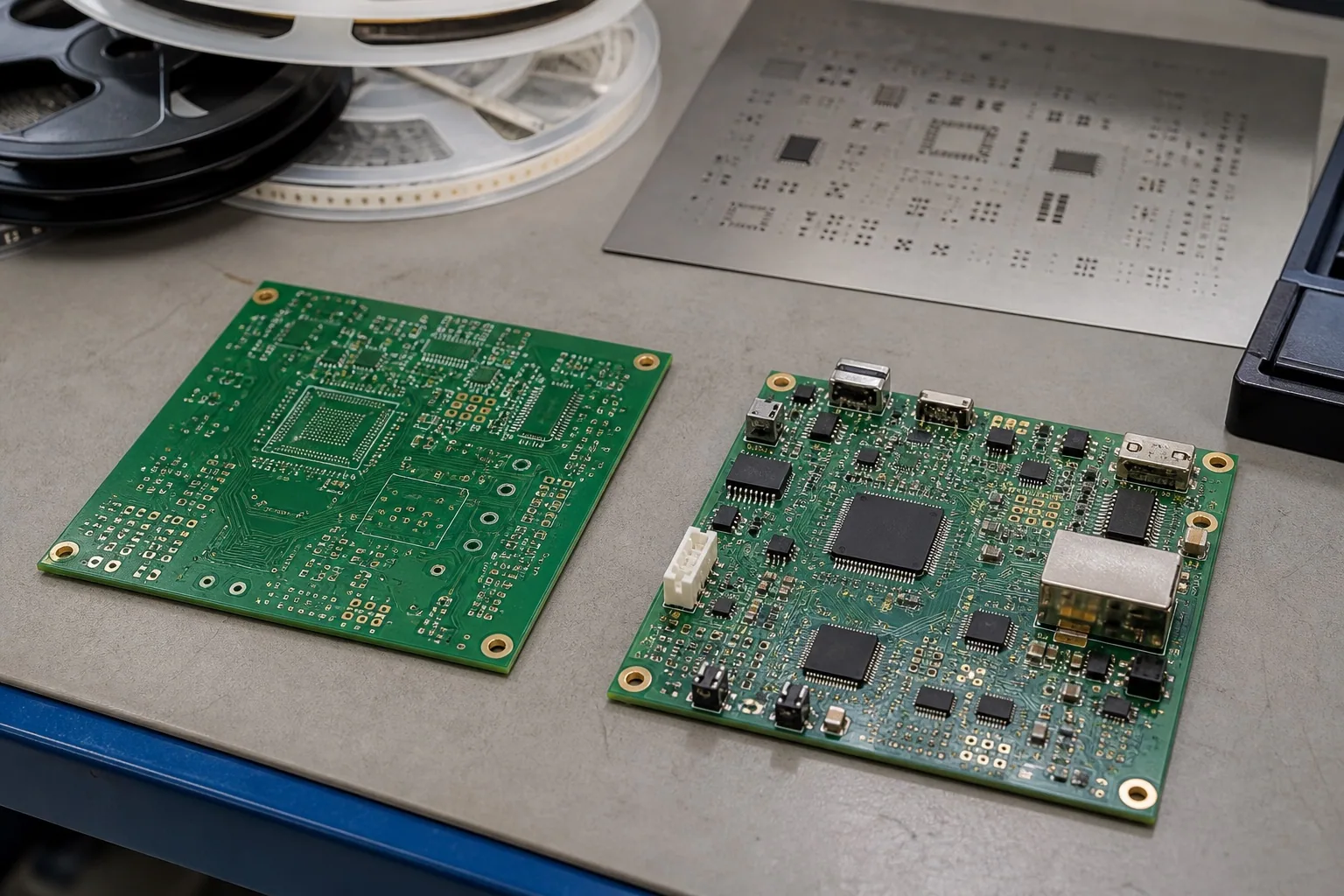
PCB vs PCBA: What's the Difference?
Learn the practical difference between a bare PCB and a PCBA, including process, files, cost, lead time and when to order each.
Read article →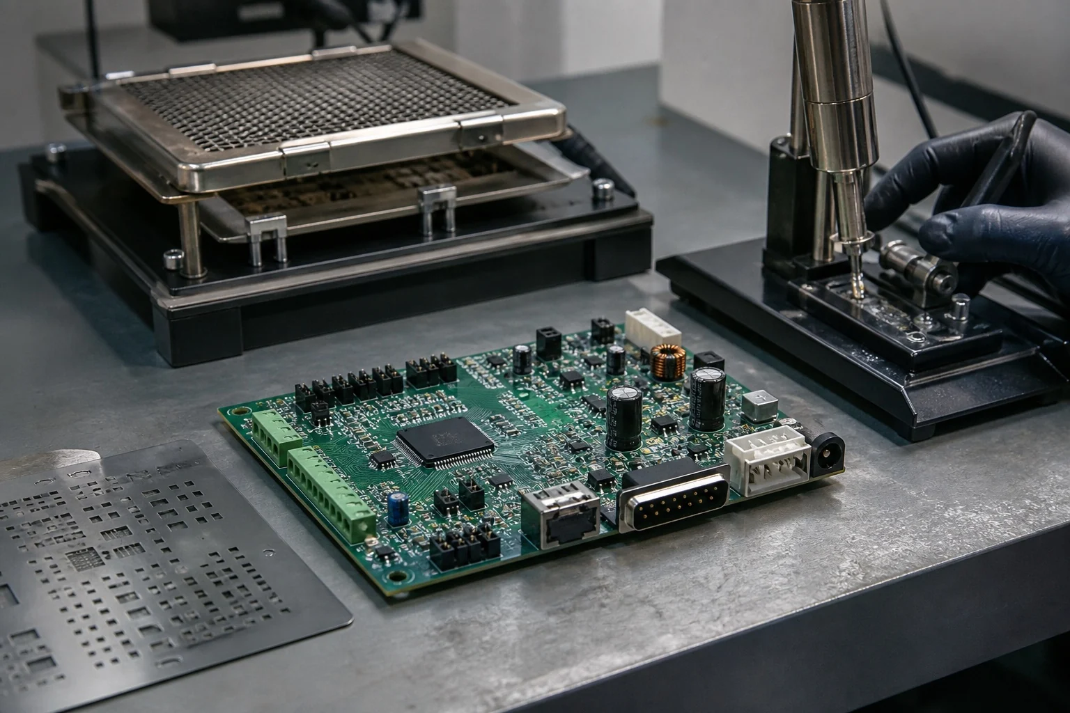 AI-generated illustration
SMT vs Through-Hole Assembly: Which Fits Your PCB?
Compare SMT and through-hole assembly by component type, board space, mechanical loads, cost and inspection. Learn when a mixed-technology build makes sense.
Read article →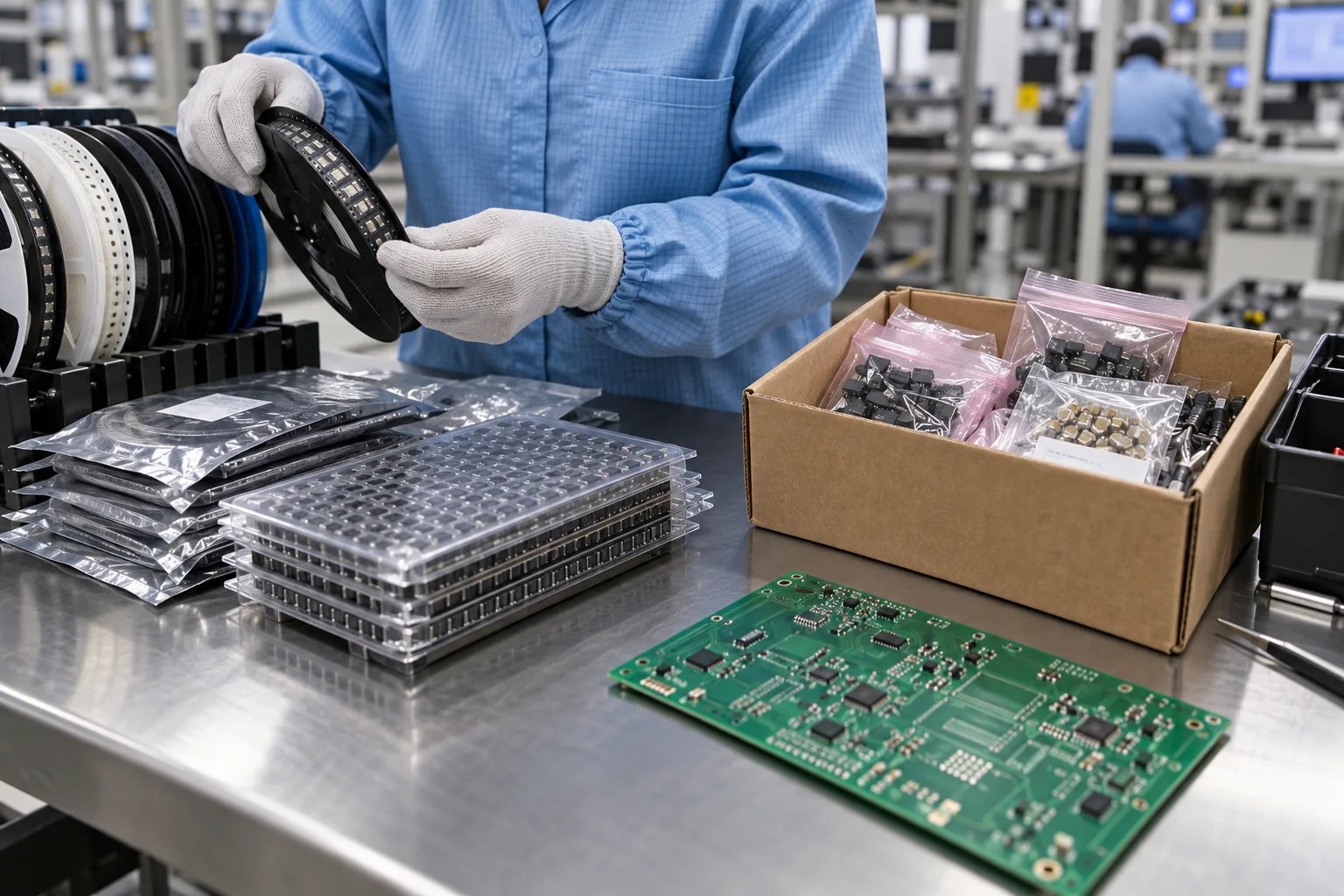 AI-generated illustration
Turnkey vs Consigned PCB Assembly: Choose by BOM Responsibility
Compare full turnkey, partial turnkey and consigned PCBA by who buys each component, approves changes, handles shortages and owns the material record.
Read article →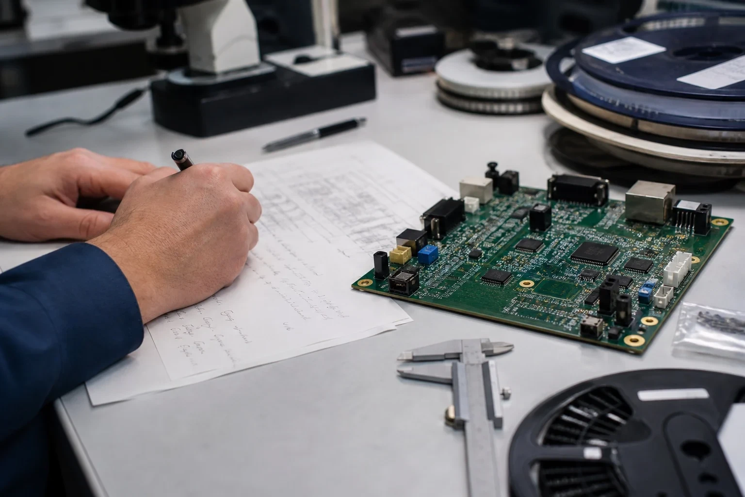
PCB Manufacturers in China: Supplier Comparison Guide
Compare PCB manufacturers in China by product fit, sourcing model and project questions, with named supplier examples and a practical shortlist checklist.
Read article →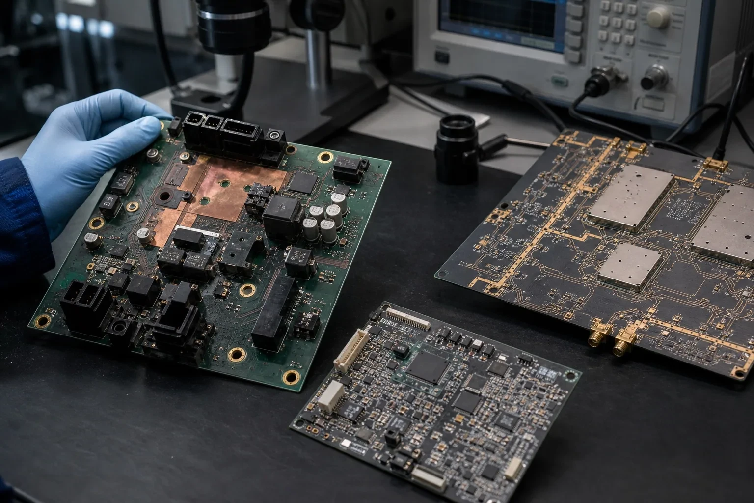
PCB Import Order Documents and Shipping Handoff
Prepare a PCB import order with a revision manifest, named commercial parties, inspection documents, packing requirements and a written freight handoff.
Read article →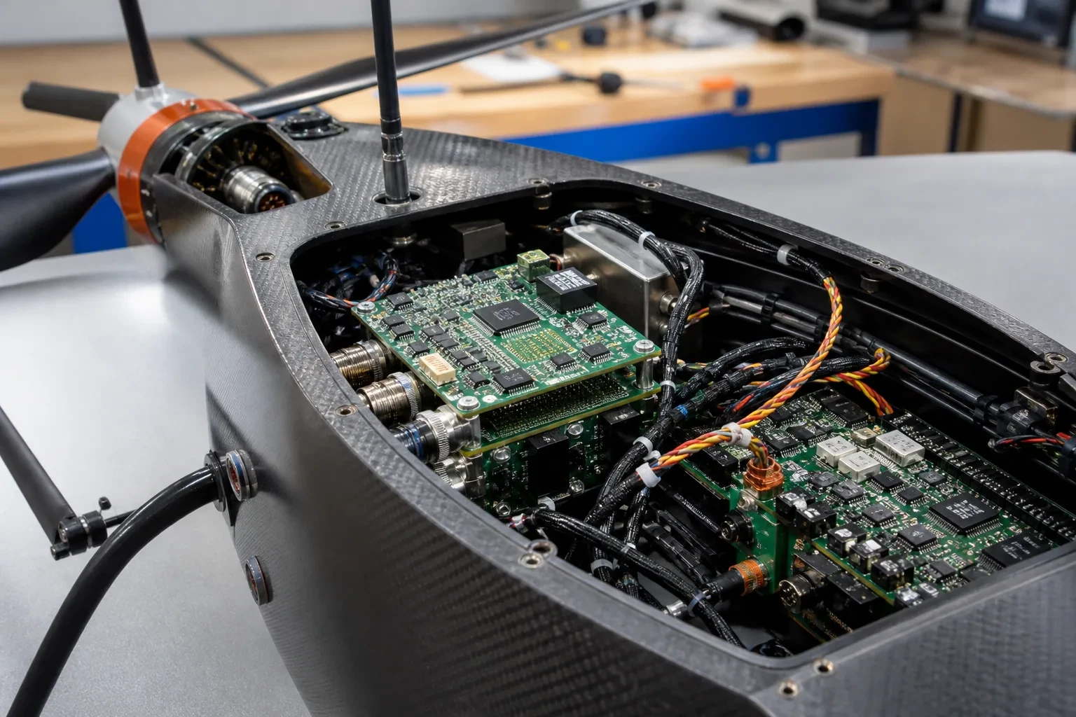
High-Reliability PCB Suppliers in China: A Project-Specific Review
Qualify PCB or PCBA suppliers for medical, aerospace and defense work by program requirements, site-specific quality evidence, materials, inspection and release records.
Read article →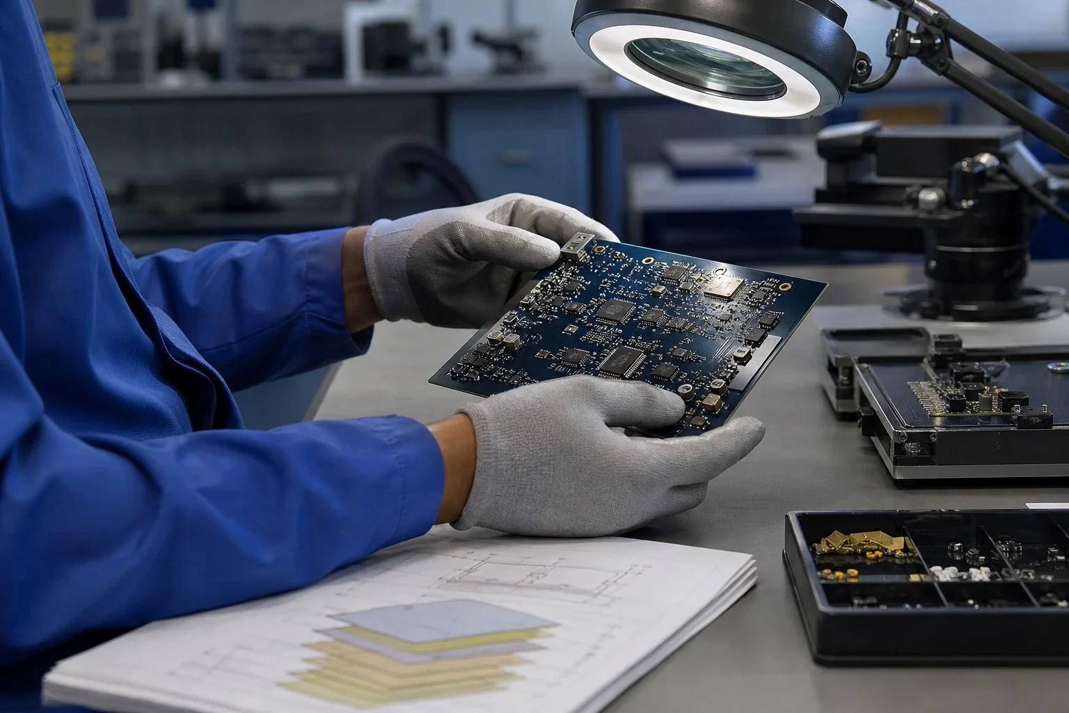
How to Verify ISO and IATF Claims from PCB Suppliers in China
Check the certificate holder, production site, process scope and current status before treating a PCB supplier’s ISO or IATF claim as relevant to your build.
Read article →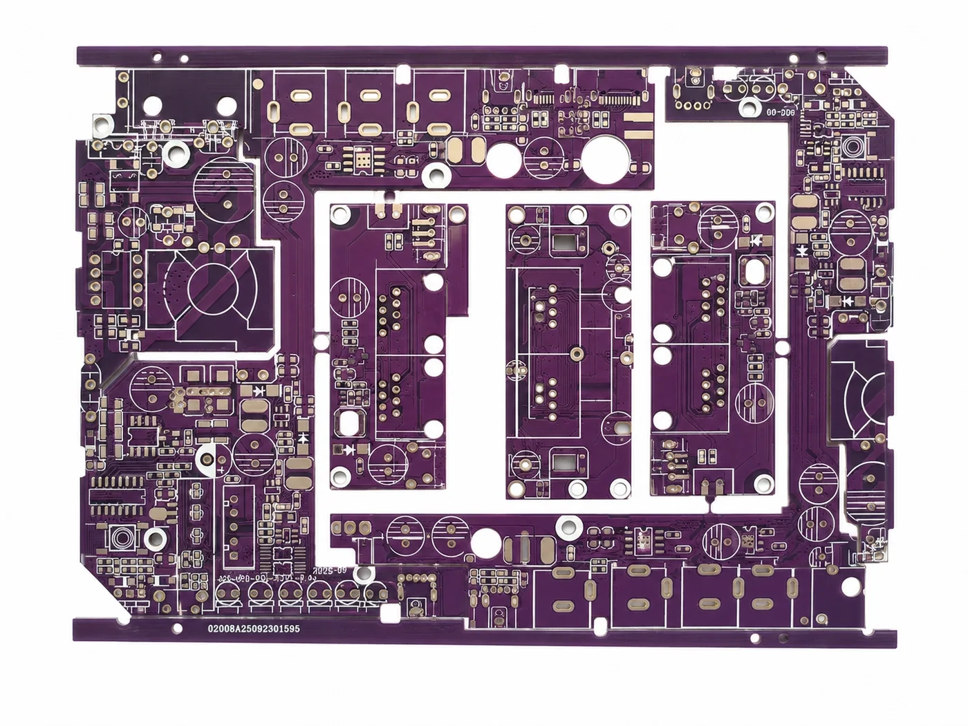
Quick-Turn PCB Prototypes in China: Compare the Actual Schedule
Choose a quick-turn PCB prototype supplier by file readiness, material availability, DFM review, committed production dates and the handoff to repeat builds.
Read article →
One-Stop PCBA Providers in China: Define the Scope First
Compare one-stop PCBA quotations by who owns PCB fabrication, component sourcing, assembly, testing, documentation and changes for your project.
Read article →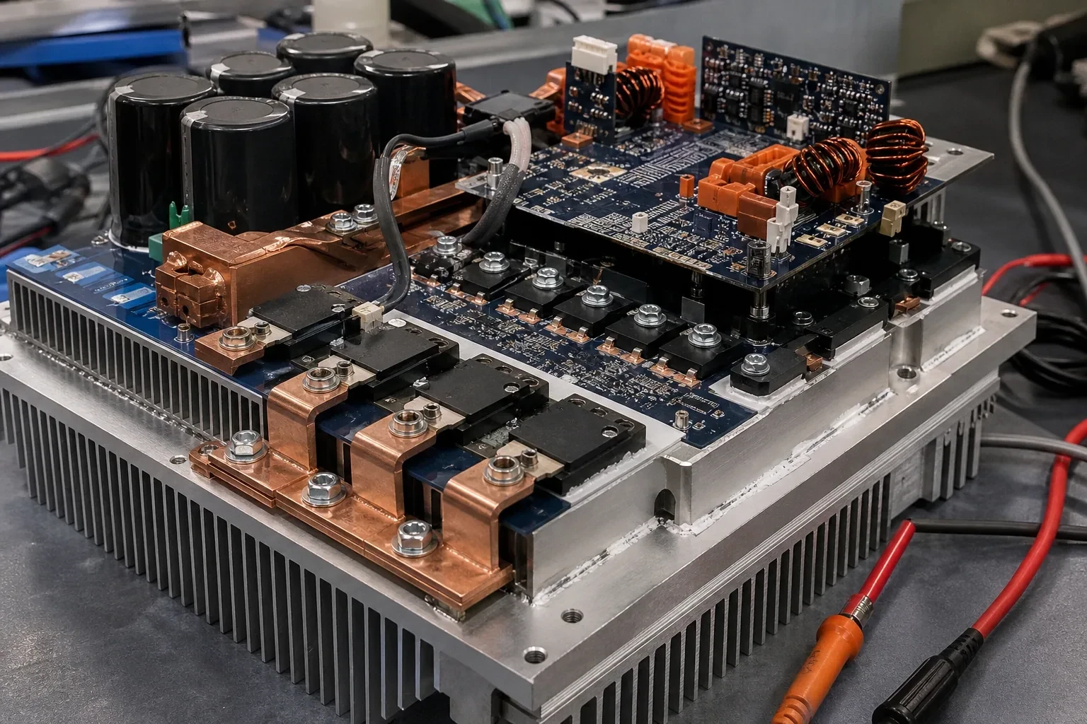
Automotive PCB Suppliers in China: What Buyers Should Verify
Evaluate an automotive PCB or PCBA supplier by the actual production site, IATF scope, PPAP responsibility, traceability and change-control plan for your program.
Read article →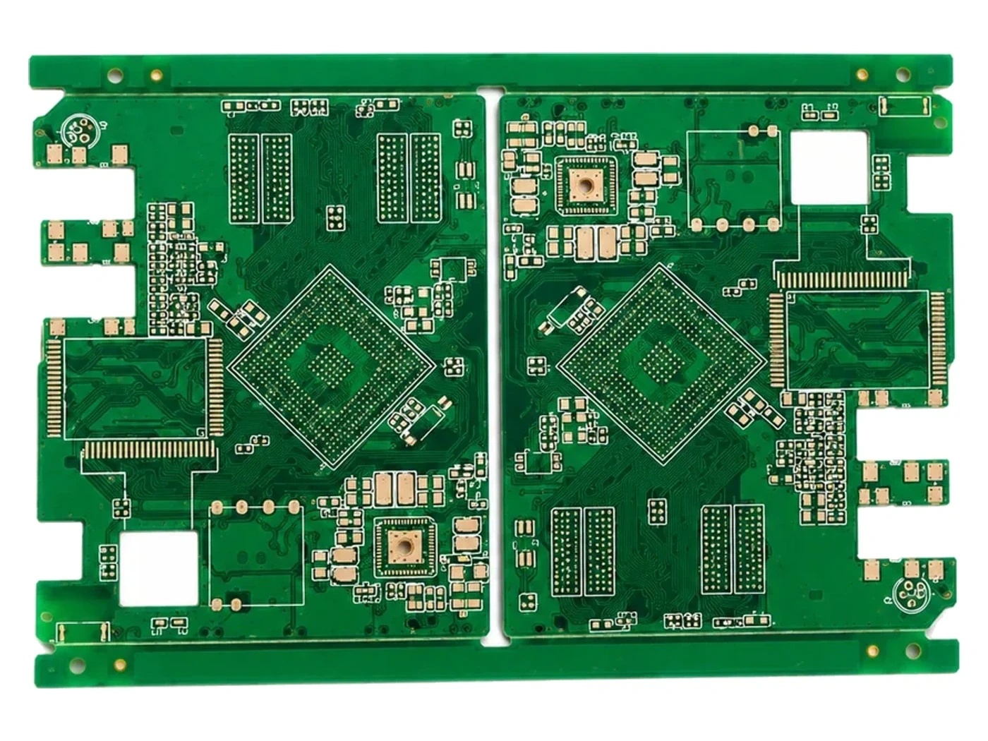
How to Evaluate HDI and Multilayer PCB Suppliers in China
Review HDI and multilayer PCB suppliers by the stackup, microvia route, impedance plan, manufacturing limits and inspection evidence for your design.
Read article →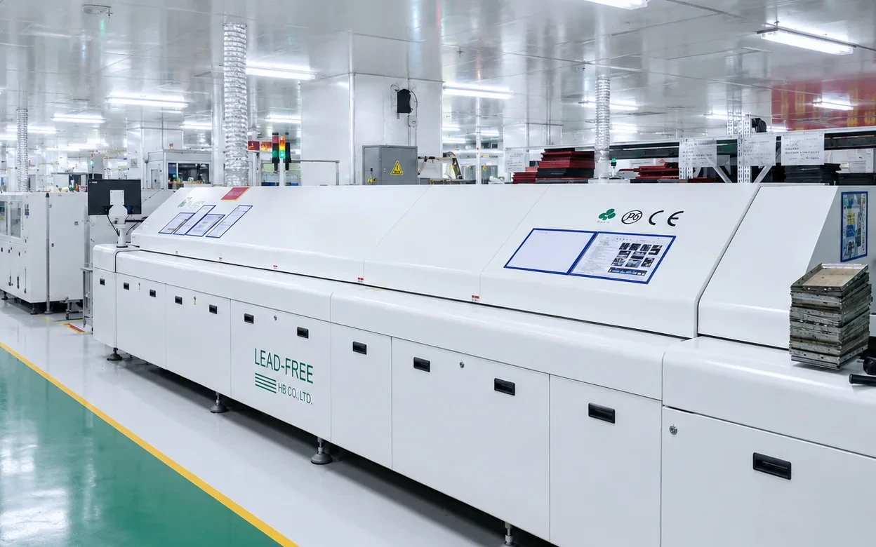
High-Volume PCB Manufacturers in China: Buyer Guide
Compare high-volume PCB manufacturers in China through supplier examples, recurring-order questions, material continuity and lot-level acceptance requirements.
Read article →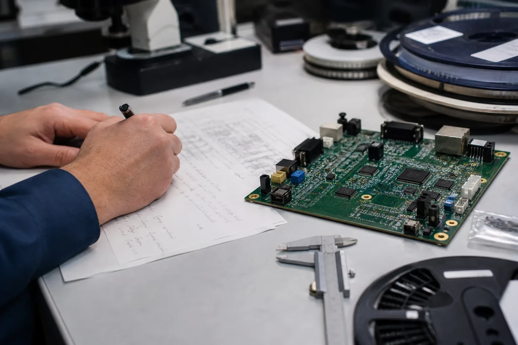
Compare International PCB Quotes Before Ordering
Compare international PCB quotations on the same revision, manufacturing scope, tooling, tests, freight and exclusions before choosing an order.
Read article →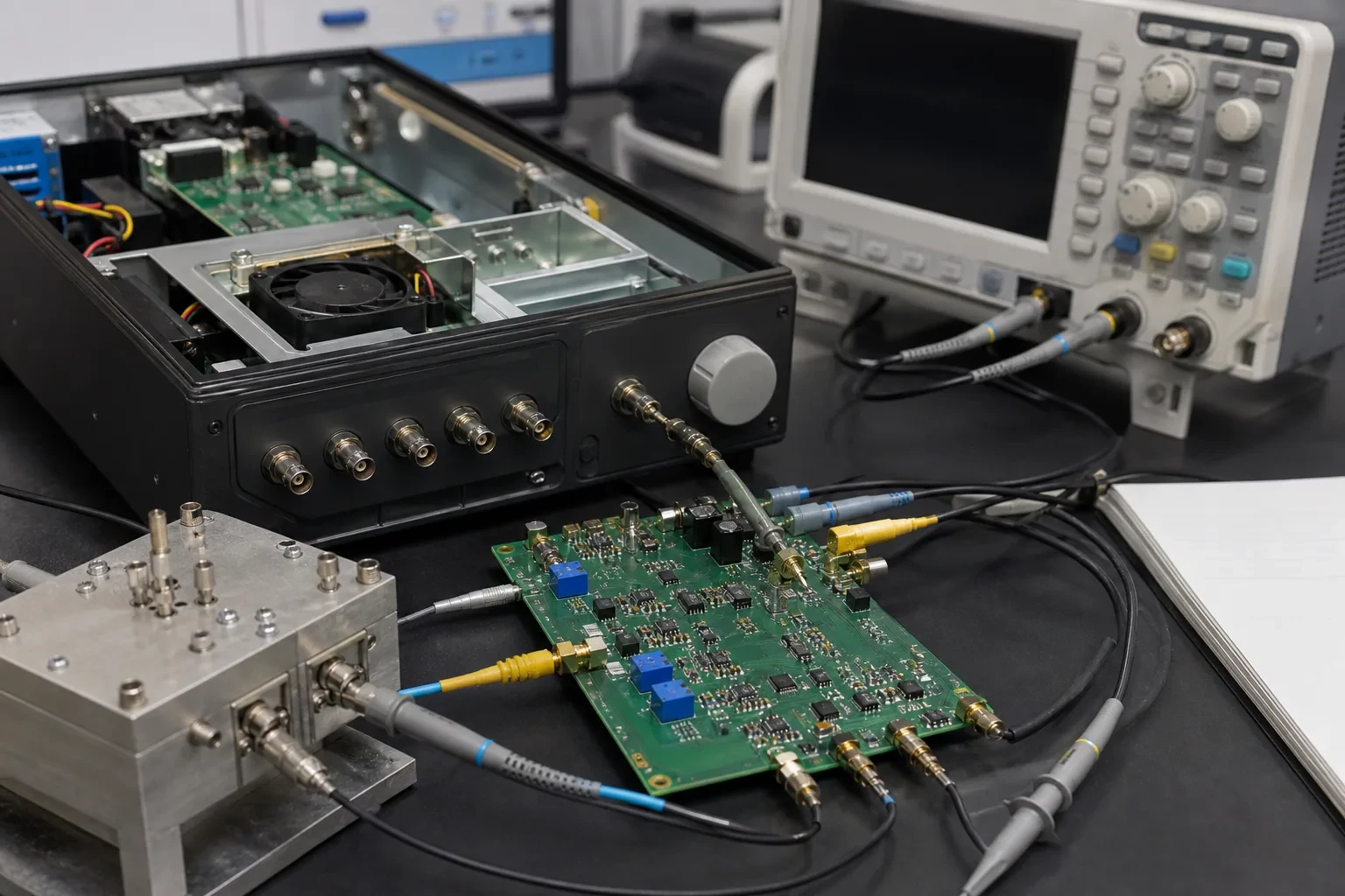
PCB Inspection Methods: SPI, AOI, X-Ray, ICT & FCT
Compare PCB inspection methods including SPI, AOI, X-ray, ICT, flying probe and functional test, and see where each fits in PCBA production.
Read article →Related resource pages
Keep the article open while you validate the build.
Have a project in mind?
Upload your Gerber files, BOM, or project requirements.
Our engineering team reviews every inquiry personally — no automated pricing.
YOUR DESIGN FILES ARE PROTECTED UNDER STRICT CONFIDENTIALITY PROCEDURES. NDA AVAILABLE UPON REQUEST.Get a Quote →Contact Us