
1+N+1
One microvia layer per side for a cost-conscious transition from conventional multilayer.
HDI PCB manufacturing supports fine-pitch escape routing and compact board geometry through laser microvias, sequential lamination and a reliability-focused via structure.
More sequential lamination is not automatically better. The right structure achieves fanout and signal goals without adding avoidable process risk.
One microvia layer per side for a cost-conscious transition from conventional multilayer.
Two sequential lamination cycles for denser BGA escape and more routing freedom.
Advanced processors, RF modules and highly constrained interconnect.
Microvia connectivity between layers for designs that cannot use a fixed buildup.
The values below describe available advanced capability, not a promise that every limit can be combined on one board.
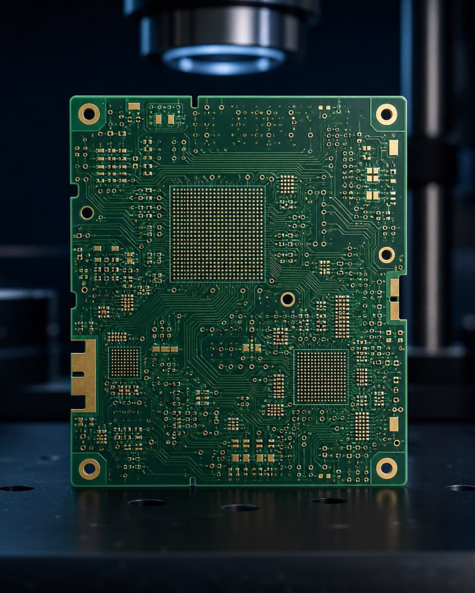
R&D prototype and high-end HDI builds
| Layer count | Up to 64 layers for prototype / engineering builds |
|---|---|
| Minimum trace / spacing | 2 / 2 mil (0.05 / 0.05 mm) |
| Standard mechanical drill | 0.15 mm |
| Advanced / special hole capability | Down to 0.10 mm, subject to design and process review |
| Minimum laser microvia | 0.075 mm |
| Aspect ratio | Up to 20:1 for qualified designs; 15:1 or below for standard advanced production |
| HDI structures | 1+N+1, 2+N+2, multi-step HDI and Any-Layer HDI |
| Via technology | Blind vias, buried vias, stacked vias, staggered vias, via-in-pad, VIPPO / POFV, resin-filled and plated-over vias |
| Sequential lamination | Supported |
| Any-layer interconnection | Supported |
| Back drilling | Supported |
| Controlled impedance | ±10% standard; ±5% for tighter requirements |
| Warpage control | ≤0.5% available when specified, subject to stack-up and design review |
| High-speed / high-frequency materials | Rogers, Taconic/AGC, PTFE/Teflon, F4B, High-Tg FR-4 and other low-loss specialty laminates |
Capability values are design-dependent. Material, copper weight, layer count, via structure, finished thickness and surface finish can change the achievable combination.
Stacked vias maximize density, while staggered structures can reduce stress. Via-in-pad supports fine-pitch BGA fanout but requires controlled filling and planarization.
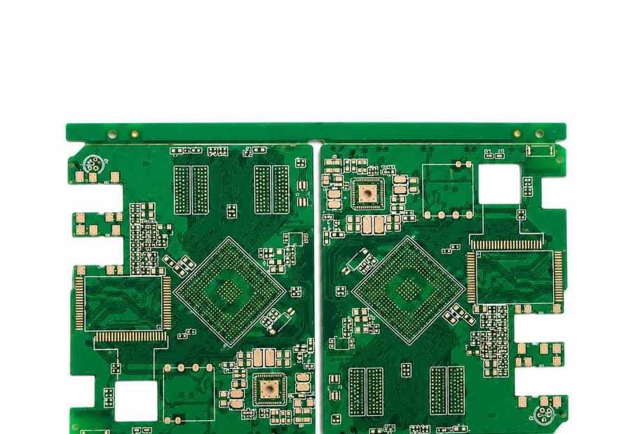
Confirm microvia geometry, capture pads, filling, stacking and dielectric thickness before the HDI production package is frozen.
Use these examples as a starting point. The board construction still follows the product’s electrical, mechanical and qualification requirements.
Wearables and space-constrained consumer devices.
Dense fanout for packages at 0.4 mm pitch and below.
DDR, PCIe and SerDes channels with controlled transitions.
Modules requiring compact routing and controlled impedance.
Portable diagnostic and imaging electronics.
ADAS, camera and sensor modules with high interconnect density.
Quality documents
The published ISO records name Zhongshan Wenquan Electronic Manufacturing Co., Ltd. and its Zhongshan PCBA facility. They do not certify every PCBArise facility, service or product.
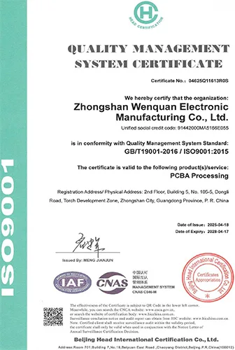
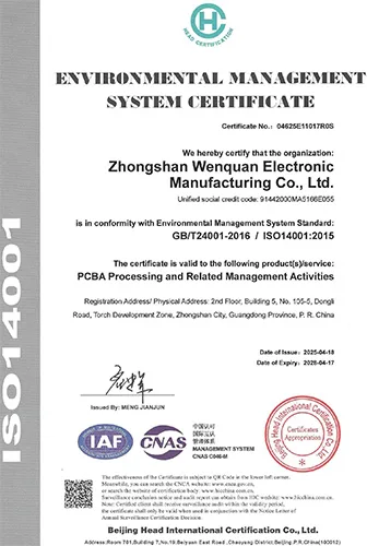
These are management-system certificates, not product or batch COAs. No batch inspection reports or COAs are currently published here.
These answers address common HDI structure, microvia, impedance and manufacturability decisions.
Advanced HDI builds can use a 0.075 mm laser drill. The capture pad, dielectric thickness and microvia aspect ratio still require stackup-level confirmation.
Yes, any-layer interconnection is available for designs that need microvia connectivity throughout the buildup. It receives a dedicated engineering and lamination review.
A 1+N+1 structure is the usual entry point. Engineering should only add sequential layers when escape routing or signal requirements justify them.
Material Dk, dielectric thickness, copper geometry and finished thickness are modeled together. ±5% control is available for tighter requirements on qualified advanced builds.
Compare HDI with conventional multilayer construction, published process limits, DFM review and prototype validation.
Share the available Gerber, ODB++, drawing, stackup or project requirements with the PCBArise team.