
Single-board and small-batch prototype
A single-board or small-batch prototype request can be quoted against the actual construction and panelization.
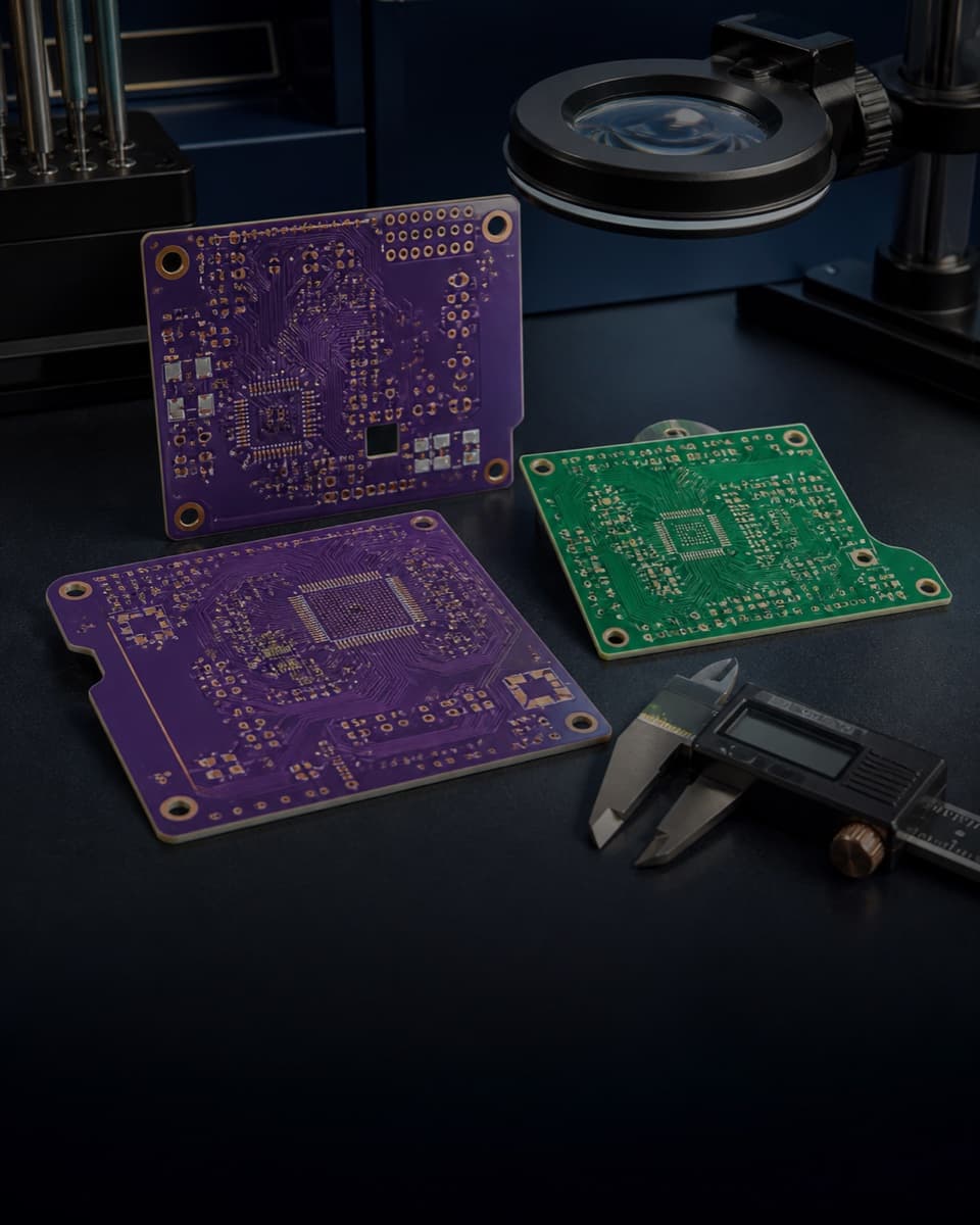
Prototype PCB manufacturing turns approved design data into production-intent boards for fit, electrical, assembly and engineering validation. Quick-turn PCB fabrication and fast-turn PCB manufacturing options are reviewed against the released package, materials, process requirements and testing plan.
Prototype value comes from using the intended stackup, material and process—not from building a reduced-spec sample that must be requalified later.
A single-board or small-batch prototype request can be quoted against the actual construction and panelization.
Resolve geometry, stackup and file-package questions before the clock starts.
Use the stackup and material system intended for later production.
Confirm electrical test, inspection and any application-specific acceptance requirements with the build.
The schedule is confirmed after production data, materials, lamination, special processes and testing requirements are reviewed together.
Confirmed for the actual build during quotation
| File approval | Timing starts after the production package is reviewed and approved. |
|---|---|
| Layer and lamination | Additional layers and sequential lamination extend the manufacturing path. |
| Material availability | Specialty laminates require material and supplier confirmation. |
| Special processes | Controlled impedance, back drilling and special finishes affect scheduling. |
| Testing requirements | Custom electrical, impedance or application testing is scheduled with the build. |
Same standard process window used for production
| Layer count | 1–40 layers |
|---|---|
| Base materials | FR-4, High-Tg FR-4, halogen-free FR-4, Rogers, Taconic/AGC, PI, aluminum, PTFE/Teflon, F4B and other specialty laminates |
| Board thickness | 0.10–10.0 mm |
| Minimum trace / spacing | 2.5 / 2.5 mil (0.0625 / 0.0625 mm) |
| Minimum mechanical drill | 0.15 mm |
| Minimum laser via | 0.10 mm |
| Standard aspect ratio | Up to 15:1 |
| Copper thickness | 0.5–12 oz, depending on board type and construction |
| Controlled impedance | ±10% standard; ±5% for tighter requirements |
| Warpage | ≤0.75% standard; ≤0.5% available when specified |
| Surface finishes | HASL, Lead-Free HASL, OSP, ENIG, Immersion Silver, Immersion Tin, ENEPIG, Hard Gold, Gold Finger and selective finishes |
Capability values are design-dependent. Material, copper weight, layer count, via structure, finished thickness and surface finish can change the achievable combination.
Incomplete fabrication notes return questions. A coherent package lets engineering confirm quick-turn PCB fabrication, quotation and production release with fewer revision loops.
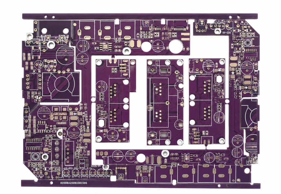
Confirm file completeness, revision alignment, materials, testing and acceptance criteria before the prototype PCB schedule is released.
Use these examples as a starting point. The board construction still follows the product’s electrical, mechanical and qualification requirements.
Confirm board outline, connectors, mounting and mechanical integration.
Evaluate power, signal behavior and functional performance.
Check footprint, soldering and access before larger builds.
Use a small batch to validate process stability and field performance.
Keep approved files, stackup and material consistent into volume.
Turn test findings into a clearly controlled next design revision.
Quality documents
The published ISO records name Zhongshan Wenquan Electronic Manufacturing Co., Ltd. and its Zhongshan PCBA facility. They do not certify every PCBArise facility, service or product.
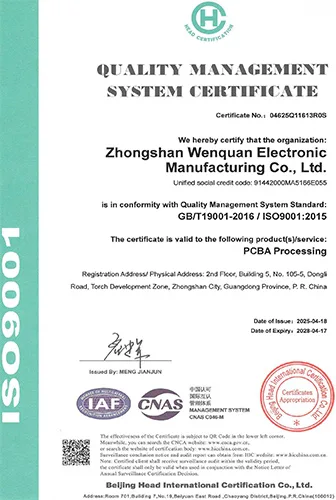
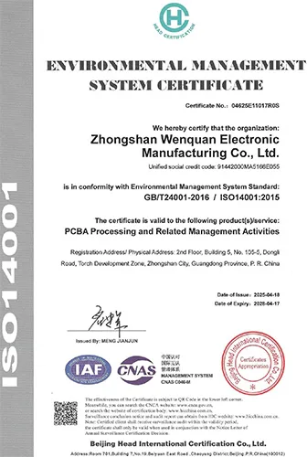
These are management-system certificates, not product or batch COAs. No batch inspection reports or COAs are currently published here.
These answers cover prototype quantity, production-intent construction, schedule drivers and the path to scale.
Single-board and small-batch prototype requests can be evaluated and quoted against the construction, panelization and process requirements. Final order quantity is confirmed with the build.
A quick-turn PCB is a bare board manufactured on an accelerated route after the production files, material, process and acceptance requirements are approved. Timing is confirmed from the actual build rather than a generic promise.
Prototype PCB timing is confirmed after file approval and depends on material availability, layer count, lamination cycles, special processes and testing requirements.
The prototype uses the intended production stackup and process controls so that successful validation can move forward without a reduced-spec requalification step.
Incomplete fabrication notes, unresolved DFM findings, material availability and complex lamination or special processes are common schedule drivers.
Move from a validated prototype to DFM closure, capability confirmation, pilot production and volume release.
Share the available Gerber, ODB++, drawing, stackup or project requirements with the PCBArise team.