
5G cellular base-station radio units, remote radio units and small cells
Industries / PCB & PCBA
Telecom PCB Assembly & RF PCB Manufacturer
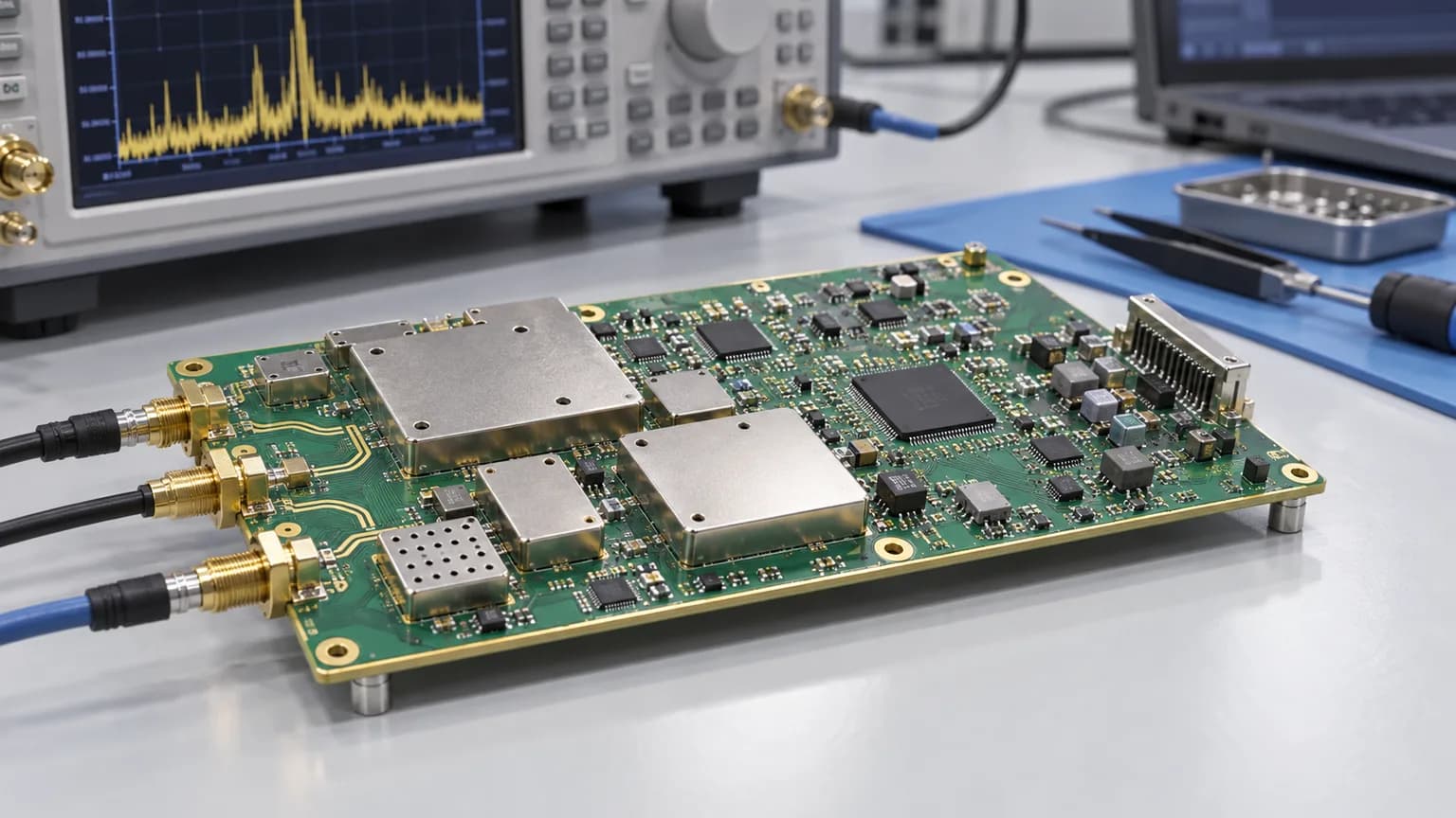
PCBArise provides telecom PCB assembly and RF PCB manufacturing for 5G base-station radio units, small cells, transceivers, antenna interfaces, network switches, wireless gateways and high-speed communication equipment. The buyer’s product—radio, backplane, power, filter or edge-network module—sets the loss budget, stackup, impedance, shielding, thermal and assembly evidence that must be held.
Controlled ImpedanceRF Materials ReviewHDI OptionsAOI / X-Ray / ICT
Product useTelecom PCB Assembly for 5G Base Stations, Transceivers & RF ModulesChosen for your product
Board constructionHigh-Frequency 5G & Controlled-Impedance PCB
Assembly routeTelecom PCB Assembly for 5G Base Stations, Transceivers & RF Modules
Quality checksTelecom RF Quality, Impedance & Test Evidence
Typical applications
Telecom PCB Assembly for 5G Base Stations, Transceivers & RF Modules
Telecom buyers search for a PCB supplier around the radio or network product they are releasing. We identify whether the board is an RF front end, transceiver, antenna interface, base-station control card, power board or high-speed backplane before quoting.
RF transceiver, antenna-interface, filter, amplifier and front-end boards
Microwave, wireless backhaul and private-5G communication equipment
Network switches, routers, gateways and high-speed backplanes
Industrial wireless, edge-network and telecom power/control electronics
Satellite communication and ground-terminal electronics where project scope permits
Engineering choices
What RF and Telecom PCB Buyers Need to Qualify
RF performance is a product-level promise. A small stackup, material, connector, shielding or assembly change can move the radio match, insertion loss or high-speed margin, so the quote starts with the released RF and network requirements.
RF loss budget: dielectric thickness, Dk/Df, copper roughness and stackup stability affect the radio path
5G and high-speed return paths: differential impedance, length, ground and shielding decisions stay linked
Base-station reality: thermal density, outdoor enclosure, coating, corrosion and connector access matter
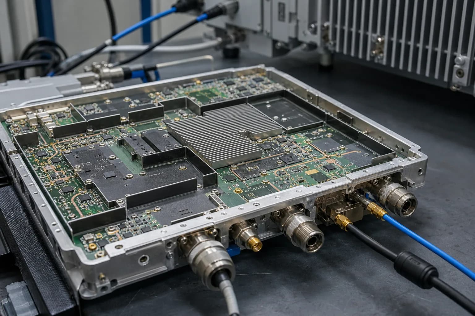
RF module assembly: fine-pitch packages, shielding cans, coax connectors and heat spreaders need fixture access
Production repeatability: material lot, finish, soldering, stackup and impedance records must match the release
Board and process options
High-Frequency 5G & Controlled-Impedance PCB
The RF front end, transceiver or backplane determines the advanced stackup, HDI, microvia, back-drilling and impedance route. Final geometry is confirmed against the frequency range, loss budget, layer assignment and released field-solver data.
Product focus
RF performance is protected by stackup discipline and measurable evidence.
Base-station, transceiver and network boards need the released dielectric, impedance, return-path, shielding and thermal decisions to survive fabrication and assembly.
- RF material and loss budget
- Controlled impedance and back drilling
- Shielding, thermal and test access
Advanced Multilayer & HDI PCB
R&D prototyping and high-end HDI builds
| Parameter | Specification |
|---|---|
| Layer Count | Up to 64 Layers(Prototype / engineering builds) |
| Min Trace Width / Spacing | 2 / 2 mil (0.05 / 0.05 mm) |
| Standard Mechanical Drill | 0.15 mm |
| Advanced / Special Hole Capability | Down to 0.10 mm, subject to design and process review |
| Min Laser Microvia | 0.075 mm |
| Aspect Ratio | Up to 20:1 for qualified designs; 15:1 or below for standard advanced production |
| Controlled Impedance | ±10% standard; ±5% for tighter requirements |
| HDI Structures | 1+N+1, 2+N+2, multi-step HDI and Any-Layer HDI |
| Via Technology | Blind vias, buried vias, stacked vias, staggered vias, via-in-pad, VIPPO / POFV, resin-filled and plated-over vias |
| Sequential Lamination | Supported |
| Any-Layer Interconnection | Supported |
| Back Drilling | Supported |
| Warpage Control | ≤0.5% available when specified, subject to stack-up and design review |
| High-Speed / High-Frequency Materials | Rogers, Taconic/AGC, PTFE/Teflon, F4B, High-Tg FR-4 and other low-loss specialty laminates |
| Board Thickness Tolerance | ±0.05 mm |
| Thermal Conductivity | Up to 3.0 W/m·K(Aluminum PCB) |
Assembly considerations
Materials for RF Front Ends & Telecom Backplanes
Rogers, Taconic, PTFE/Teflon, High-Tg FR-4 and other approved materials are considered for the radio, antenna interface, base-station backplane or network module. Dielectric loss, thermal behavior, availability, finish and copper roughness follow the product requirement.
Options to discuss
Start with what your design needs.
We can confirm the workable combination after reviewing your files.
RogersTaconicHigh-Tg TG170FR-4PTFE / TeflonENIGENEPIGImmersion SilverOSPBack DrillingVia-in-PadShielding
What to send
Choose for the product you are building.
- RF material and loss budget
- Controlled impedance and back drilling
- Shielding, thermal and test access
Board and process options
RF Transceiver, Base-Station & Network PCBA
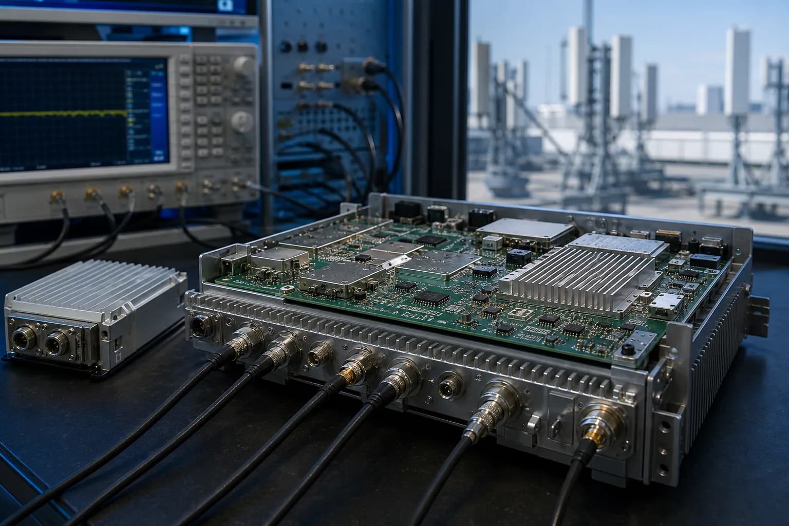
Fine-pitch RF processors, connectors, shielding, heat spreaders and mixed-technology content are assembled to the approved radio or network module package, stencil, reflow, inspection and test requirements.
Product focus
RF performance is protected by stackup discipline and measurable evidence.
Base-station, transceiver and network boards need the released dielectric, impedance, return-path, shielding and thermal decisions to survive fabrication and assembly.
- RF material and loss budget
- Controlled impedance and back drilling
- Shielding, thermal and test access
PCB Assembly Specifications
SMT, THT and mixed technology assembly capabilities
| Parameter | Specification |
|---|---|
| Min Component Size | 01005 (0.4 × 0.2 mm) |
| Component Size Range | 01005 to 150 × 100 × 30 mm |
| Min BGA Pitch | 0.25 mm |
| Min QFP / QFN Pitch | 0.15 mm spacing / 0.3 mm width |
| Placement Accuracy (X/Y) | ±0.025 mm (±25 μm) |
| Placement Accuracy (θ) | ±0.2° |
| Max BGA Component Size | 70 × 74 mm |
| Max PCB Assembly Size | 400 × 1200 mm(Min 50 × 50 mm; applicable process-line envelope, subject to board support and panelization review) |
| PCB Thickness Range | 0.3–10.0 mm |
| Warpage Control | ≤0.5%(Subject to board construction and assembly process review) |
| Max Component Height | 120 mm(Applicable equipment and assembly route; confirm package clearance during engineering review) |
| Soldering Methods | Wave Soldering, Selective Soldering, Hand Soldering |
| Reflow Atmosphere | Air / Nitrogen(Nitrogen reflow on applicable lines; oxygen target depends on the assembly route and profile) |
| SMT Production Capacity | 700+ million points / month(Combined figure across 20+ SMT lines; not a per-facility or per-line guarantee) |
How the board fits the product
RF performance is protected by stackup discipline and measurable evidence.
Base-station, transceiver and network boards need the released dielectric, impedance, return-path, shielding and thermal decisions to survive fabrication and assembly.
- RF material and loss budget
- Controlled impedance and back drilling
- Shielding, thermal and test access
Controlled ImpedanceRF Materials ReviewHDI OptionsAOI / X-Ray / ICT
Inspection, testing and records
Telecom RF Quality, Impedance & Test Evidence
The evidence plan follows the RF or network product: stackup and impedance calculations, dimensional and visual inspection, SPI/AOI/X-ray, electrical coverage, programming and project-specific RF or high-speed acceptance checks. Quality-system, material and traceability records are tied to the approved scope.
ISO 9001:2015ISO 14001:2015
Build files
Keep the board revision, BOM and assembly drawings together so the factory builds the intended configuration.
Inspection and test
Choose optical, X-ray, electrical or functional checks for the defects that matter to this product.
Material tracking
Agree which material and production records you need to retrieve after shipment.
Design changes
Decide who can approve a material, component or process change before it reaches the line.
Quality documents
Preview & download certificates
The published ISO records name Zhongshan Wenquan Electronic Manufacturing Co., Ltd. and its Zhongshan PCBA facility. They do not certify every PCBArise facility, service or product.
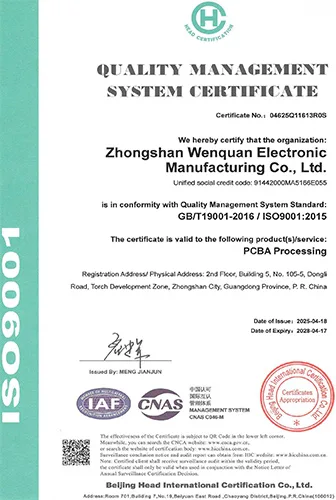
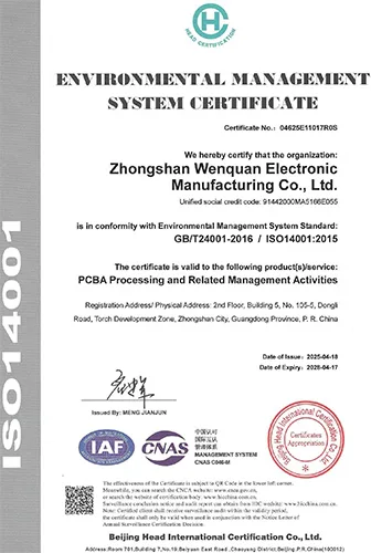
These are management-system certificates, not product or batch COAs. No batch inspection reports or COAs are currently published here.
Frequently asked questions
Common questions about this PCB application
Start with the board, environment and files you have; the detailed route depends on your design.
Can you manufacture RF and telecom PCBs with controlled impedance?
Yes. Controlled impedance, stackup review, material selection, trace geometry, return paths, and production tolerances are reviewed against the released design. Standard and strict impedance references are available, but the final tolerance is confirmed for the actual stackup and frequency.
Which materials do you use for high-frequency PCB projects?
Rogers, Taconic, PTFE/Teflon, High-Tg FR-4, and other approved constructions can be considered. The choice depends on loss, Dk/Df, thermal profile, copper roughness, availability, and the RF acceptance requirement.
Can you provide telecom PCB assembly for base stations and small cells?
Yes. We support radio, transceiver, power, control, interface, and network electronics used in base-station and small-cell equipment. Send the RF stackup, thermal, shielding, connector, and test requirements so engineering can confirm the route.
Can you assemble shielded RF modules and fine-pitch packages?
Yes. Fine-pitch SMT, BGA/QFN, connectors, shielding cans, mixed technology, and selected hand or selective soldering are supported. The stencil, reflow, inspection, rework, and shield-attachment requirements are confirmed per project.
How do you verify RF PCB quality?
Fabrication and assembly evidence can include stackup and impedance calculations, dimensional and visual inspection, SPI/AOI, X-ray, electrical test, ICT/FCT, and project-specific RF or high-speed checks. The exact acceptance record is agreed before release.
Can you handle telecom designs with confidentiality or export restrictions?
NDA and project confidentiality requirements can be reviewed. If a project includes controlled technical data, restricted end use, or export obligations, the applicable entity, data-handling, and compliance review must be completed before files are released for manufacturing.
Related PCB pages
Explore the board and assembly options behind this product.
Use the related PCB, PCBA and quality pages to plan the next part of your build.
PCBArise resource
High Frequency PCB
Rogers, Taconic, PTFE, stackup, and impedance references.
PCBArise resourceHDI PCB
Microvia and high-density routing for RF modules.
PCBArise resourcePCB Materials & Stackup
Material, stackup, and controlled-impedance review.
PCBArise resourcePCB Assembly Capabilities
Fine-pitch assembly and inspection options.
PCBArise resourceQuality Control
Inspection, testing, and documented release controls.
Review the RF stackup before the first production panel.
Send the frequency range, stackup, impedance targets, material list and RF acceptance plan for engineering review.