
AC and DC EVSE charging-station control, metering, communication and power boards
Industries / PCB & PCBA
EV Charger, BMS & Energy PCB Manufacturer
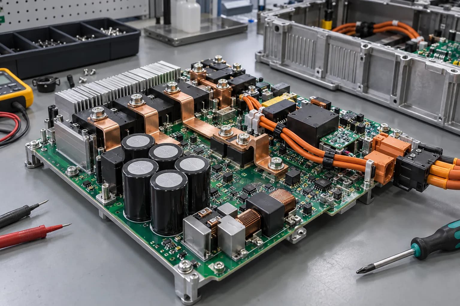
PCBArise manufactures PCB and PCBA for EVSE charging stations, on-board chargers, BMS, DC-DC converters, traction inverters, energy-storage systems and renewable-energy controls. The same quote may include high-current power, cell sensing, isolation, communication and outdoor service requirements, so the route is split by vehicle-mounted, charging-infrastructure or grid-side product scope before production is planned.
Project-specific quality scope0.5–12 oz CopperUp to 3.0 W/m·KMES Traceability
Product useEVSE, BMS, OBC & Energy-Storage PCB ApplicationsChosen for your product
Board constructionEV Charger and BMS PCB Construction
Assembly routeEVSE, BMS & Power-Conversion PCBA
Quality checksEV and Energy Quality, Isolation & Traceability
Typical applications
EVSE, BMS, OBC & Energy-Storage PCB Applications
EV and energy buyers search for a supplier around a specific power product. We cover the vehicle, charger and grid-side electronics that sit between the battery, the power conversion stage and the communication network.
On-board charger (OBC), DC-DC converter and traction-inverter electronics
BMS cell-monitoring, master/slave, balancing and battery-pack interface boards
EV charge-point communication, payment, display and protection modules
Solar inverter, microinverter, wind converter and grid-tie interface boards
Energy-storage system (ESS) and power-conversion system (PCS) electronics
Smart-meter, energy-monitoring and renewable-energy gateway boards
Engineering choices
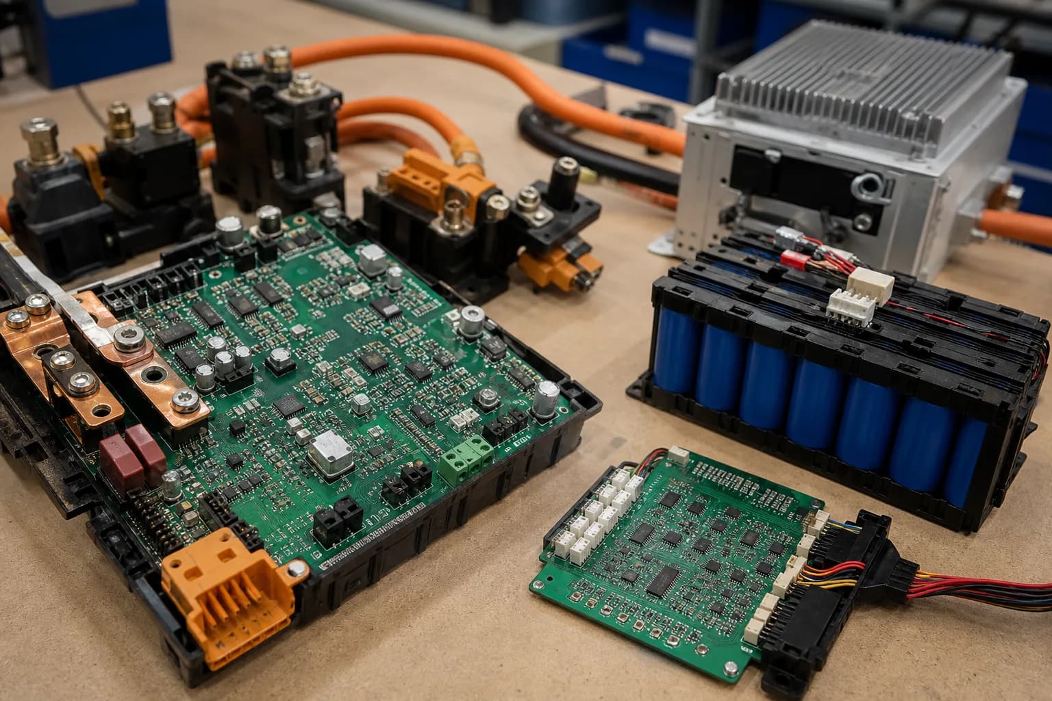
What EV and Energy PCB Buyers Need to Qualify
An EV charger or BMS PCB is both a power product and a measurement product. Buyers need a build partner who can separate vehicle-mounted quality requirements from infrastructure scope while keeping isolation, sensing, thermal and outdoor-service decisions visible.
High-voltage isolation: creepage, clearance, slots, coating and cleanliness follow the charger or pack architecture
Continuous current: copper weight, thermal path, connector rating and component placement are sized for sustained load
BMS measurement: cell sensing and current measurement must remain separated from hard-switching noise
Outdoor EVSE service: humidity, temperature swing, corrosion, enclosure and maintenance assumptions affect the board
Power cycling: solder joints, plated-through holes and high-mass components are reviewed against charge/discharge duty
Scope boundary: vehicle-mounted OBC/BMS, charging infrastructure and grid-side ESS each need their own evidence plan
Board and process options
EV Charger and BMS PCB Construction
The power path, sensing density and enclosure determine the stackup and copper. Standard rigid and multilayer PCB production covers the released EVSE, BMS and energy-control design; heavy copper, metal core and advanced builds are reviewed when the application requires them.
Product focus
EV and energy boards have to balance power, heat, safety and service life.
Charging, BMS, inverter and renewable-energy boards are reviewed as complete power systems, from current paths and insulation to test access and assembly evidence.
- High-current and thermal paths
- BMS sensing and isolation
- Charging, inverter and protection interfaces
Standard PCB Specifications
Volume production capabilities for rigid and multilayer PCB
| Parameter | Specification |
|---|---|
| Layer Count | 1–40 Layers |
| Base Material | FR-4, High-Tg FR-4, halogen-free FR-4, Rogers, Taconic/AGC, PI, aluminum, PTFE/Teflon, F4B and other specialty laminates |
| Board Thickness | 0.10–10.0 mm |
| Min Trace Width / Spacing | 2.5 / 2.5 mil (0.0625 / 0.0625 mm) |
| Min Mechanical Drill | 0.15 mm |
| Min Laser Via | 0.10 mm |
| Standard Aspect Ratio | Up to 15:1 |
| Copper Thickness | 0.5–12 oz, depending on board type and construction |
| Min BGA Pad Diameter | 8 mil |
| Controlled Impedance | ±10% standard; ±5% for tighter requirements |
| Warpage | ≤0.75% standard; ≤0.5% available when specified |
| Surface Finishes | HASL, Lead-Free HASL, OSP, ENIG, Immersion Silver, Immersion Tin, ENEPIG, Hard Gold, Gold Finger and selective finishes |
Board and process options
OBC, Inverter & Battery-Pack Thermal Options
OBC, inverter and battery-pack power stages may transfer heat into a chassis or cold plate. Aluminum PCB reaches thermal conductivity up to 3.0 W/m·K, while ceramic and advanced stackups are considered for higher density, isolation or sensing requirements.
Product focus
EV and energy boards have to balance power, heat, safety and service life.
Charging, BMS, inverter and renewable-energy boards are reviewed as complete power systems, from current paths and insulation to test access and assembly evidence.
- High-current and thermal paths
- BMS sensing and isolation
- Charging, inverter and protection interfaces
Advanced Multilayer & HDI PCB
R&D prototyping and high-end HDI builds
| Parameter | Specification |
|---|---|
| Layer Count | Up to 64 Layers(Prototype / engineering builds) |
| Min Trace Width / Spacing | 2 / 2 mil (0.05 / 0.05 mm) |
| Standard Mechanical Drill | 0.15 mm |
| Advanced / Special Hole Capability | Down to 0.10 mm, subject to design and process review |
| Min Laser Microvia | 0.075 mm |
| Aspect Ratio | Up to 20:1 for qualified designs; 15:1 or below for standard advanced production |
| Controlled Impedance | ±10% standard; ±5% for tighter requirements |
| HDI Structures | 1+N+1, 2+N+2, multi-step HDI and Any-Layer HDI |
| Via Technology | Blind vias, buried vias, stacked vias, staggered vias, via-in-pad, VIPPO / POFV, resin-filled and plated-over vias |
| Sequential Lamination | Supported |
| Any-Layer Interconnection | Supported |
| Back Drilling | Supported |
| Warpage Control | ≤0.5% available when specified, subject to stack-up and design review |
| High-Speed / High-Frequency Materials | Rogers, Taconic/AGC, PTFE/Teflon, F4B, High-Tg FR-4 and other low-loss specialty laminates |
| Board Thickness Tolerance | ±0.05 mm |
| Thermal Conductivity | Up to 3.0 W/m·K(Aluminum PCB) |
Assembly considerations
Materials for EVSE, BMS & Renewable-Energy Boards
Material, copper, finish, coating and cleanliness are selected by product role: BMS sensing, OBC power conversion, EVSE outdoor control, ESS monitoring or inverter switching. The approved stackup and environmental profile drive the final combination.
Options to discuss
Start with what your design needs.
We can confirm the workable combination after reviewing your files.
AluminumHigh-Tg TG170FR-4CeramicRogersPIENIGENEPIGImmersion SilverLead-Free HASLOSPHeavy Copper
What to send
Choose for the product you are building.
- High-current and thermal paths
- BMS sensing and isolation
- Charging, inverter and protection interfaces
Board and process options
EVSE, BMS & Power-Conversion PCBA
EV PCBA combines magnetics, busbars, electrolytic banks, power semiconductors, cell-sensing devices, connectors and communication circuitry. The production plan follows the OBC, BMS, charger, inverter or ESS assembly, including soldering method, inspection, programming, coating and functional test.
Product focus
EV and energy boards have to balance power, heat, safety and service life.
Charging, BMS, inverter and renewable-energy boards are reviewed as complete power systems, from current paths and insulation to test access and assembly evidence.
- High-current and thermal paths
- BMS sensing and isolation
- Charging, inverter and protection interfaces
PCB Assembly Specifications
SMT, THT and mixed technology assembly capabilities
| Parameter | Specification |
|---|---|
| Min Component Size | 01005 (0.4 × 0.2 mm) |
| Component Size Range | 01005 to 150 × 100 × 30 mm |
| Min BGA Pitch | 0.25 mm |
| Min QFP / QFN Pitch | 0.15 mm spacing / 0.3 mm width |
| Placement Accuracy (X/Y) | ±0.025 mm (±25 μm) |
| Placement Accuracy (θ) | ±0.2° |
| Max BGA Component Size | 70 × 74 mm |
| Max PCB Assembly Size | 400 × 1200 mm(Min 50 × 50 mm; applicable process-line envelope, subject to board support and panelization review) |
| PCB Thickness Range | 0.3–10.0 mm |
| Warpage Control | ≤0.5%(Subject to board construction and assembly process review) |
| Max Component Height | 120 mm(Applicable equipment and assembly route; confirm package clearance during engineering review) |
| Soldering Methods | Wave Soldering, Selective Soldering, Hand Soldering |
| Reflow Atmosphere | Air / Nitrogen(Nitrogen reflow on applicable lines; oxygen target depends on the assembly route and profile) |
| SMT Production Capacity | 700+ million points / month(Combined figure across 20+ SMT lines; not a per-facility or per-line guarantee) |
Assembly considerations
Charging, Battery & Energy Assembly Scope
Options to discuss
Start with what your design needs.
We can confirm the workable combination after reviewing your files.
SMT AssemblyTHT / DIP AssemblyMixed-Technology AssemblyBGA AssemblyOdd-Form ComponentsPress-FitSelective SolderingConformal CoatingIC ProgrammingCable & Harness AssemblyBox BuildComponent Sourcing
What to send
Choose for the product you are building.
- High-current and thermal paths
- BMS sensing and isolation
- Charging, inverter and protection interfaces
How the board fits the product
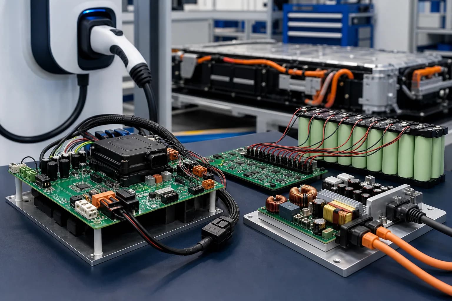
EV and energy boards have to balance power, heat, safety and service life.
Charging, BMS, inverter and renewable-energy boards are reviewed as complete power systems, from current paths and insulation to test access and assembly evidence.
- High-current and thermal paths
- BMS sensing and isolation
- Charging, inverter and protection interfaces
Project-specific quality scope0.5–12 oz CopperUp to 3.0 W/m·KMES Traceability
Inspection, testing and records
EV and Energy Quality, Isolation & Traceability
Vehicle-mounted OBC and BMS content is reviewed against the assigned facility and customer program; EVSE, ESS and renewable-energy products are scoped to their own quality and acceptance requirements. The evidence plan can include isolation and cleanliness controls, SPI/AOI/X-ray, ICT/FCT, burn-in where specified, material declarations and MES traceability.
ISO 9001:2015ISO 14001:2015
Build files
Keep the board revision, BOM and assembly drawings together so the factory builds the intended configuration.
Inspection and test
Choose optical, X-ray, electrical or functional checks for the defects that matter to this product.
Material tracking
Agree which material and production records you need to retrieve after shipment.
Design changes
Decide who can approve a material, component or process change before it reaches the line.
Quality documents
Preview & download certificates
The published ISO records name Zhongshan Wenquan Electronic Manufacturing Co., Ltd. and its Zhongshan PCBA facility. They do not certify every PCBArise facility, service or product.
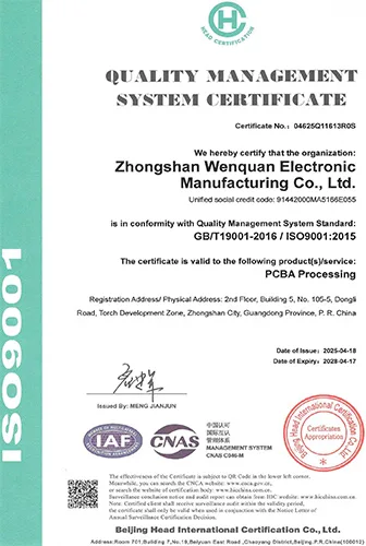
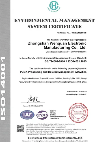
These are management-system certificates, not product or batch COAs. No batch inspection reports or COAs are currently published here.
Frequently asked questions
Common questions about this PCB application
Start with the board, environment and files you have; the detailed route depends on your design.
Do you build both vehicle-mounted and infrastructure charging electronics?
On-board chargers, DC-DC converters and BMS boards are reviewed against the applicable customer program and assigned facility. Charge posts, ESS and inverter hardware are scoped to the assigned facility, requested quality evidence and released quality plan; the RFQ confirms the documentation and process controls for the product category.
What copper weight can you build for charging and inverter power stages?
The published reference covers 0.5–12 oz copper across 1–40 layers. Copper weight follows your continuous current and allowable temperature rise. Because heavy copper etches with a trapezoidal profile, achievable trace geometry widens with copper weight — our engineers confirm the build-specific geometry during project DFM review.
Can you assemble BMS boards with high channel counts and fine-pitch front ends?
The published PCBA envelope includes 01005 (0.4 × 0.2 mm), 0.25 mm minimum BGA pitch, QFP/QFN down to 0.15 mm spacing, ±0.025 mm (±25 μm) X/Y placement accuracy and ±0.2° in θ. SPI, AOI and ICT coverage are selected against the assigned line, package mix and released quality plan; final limits are confirmed at RFQ.
How do you manage heat in charging modules and inverters?
Where conduction to the chassis is the dominant path, we move to metal core — aluminum PCB reaches up to 3.0 W/m·K thermal conductivity, and ceramic substrate is available for higher power density. On FR-4 builds, High-Tg TG170 plus thermal via design is the usual approach. Send the thermal requirement with your RFQ and engineering will recommend the construction.
Do you provide conformal coating for outdoor charging equipment?
Yes. Conformal coating is a standard value-added service, along with IC programming, cable and harness assembly, box build, and final packaging. For high-impedance sensing nodes on BMS boards we treat cleaning and coating as a functional process step, not a cosmetic one.
What traceability and testing do you provide for energy products?
MES traceability can link component, lot, process and panel records at the level agreed in the released quality plan. Testing may include 2D/3D AXI, ICT, FCT, burn-in and boundary scan/JTAG where the package, access and project acceptance plan support them; coverage and limits are confirmed before release.
Related PCB pages
Explore the board and assembly options behind this product.
Use the related PCB, PCBA and quality pages to plan the next part of your build.
PCBArise resource
Power Electronics PCB
Heavy copper and thermal management for power conversion stages.
PCBArise resourceAutomotive PCB
Vehicle-program quality, traceability and project-evidence planning.
PCBArise resourcePCB Manufacturing Capabilities
Full fabrication specifications, materials, and process limits.
PCBArise resourceTurnkey PCB Assembly
Sourcing, assembly, test, and box build from one supplier.
PCBArise resourceQuality Control
Inspection, testing, and MES traceability across the process.
Plan the EV or energy PCB build around the real power path.
Send the electrical, thermal, mechanical and test requirements for a manufacturing route review.