
Standard rigid and multilayer
The baseline process window for repeatable commercial production.
PCB manufacturing capabilities vary by material, copper weight, layer count, via structure and finished thickness. Use the applicable process window rather than combining isolated maximum values.
For stackup, finish and inspection decisions, see the PCB manufacturing guide.
The baseline process window for repeatable commercial production.
Tighter geometry, microvias and strict impedance for qualified advanced builds.
Flexible materials, coverlay, stiffeners and cycle-life considerations.
Heavy copper, metal core and controlled-Dk material systems.
The most aggressive value in one row may not combine with every other limit. Final capability is confirmed from the complete production package.
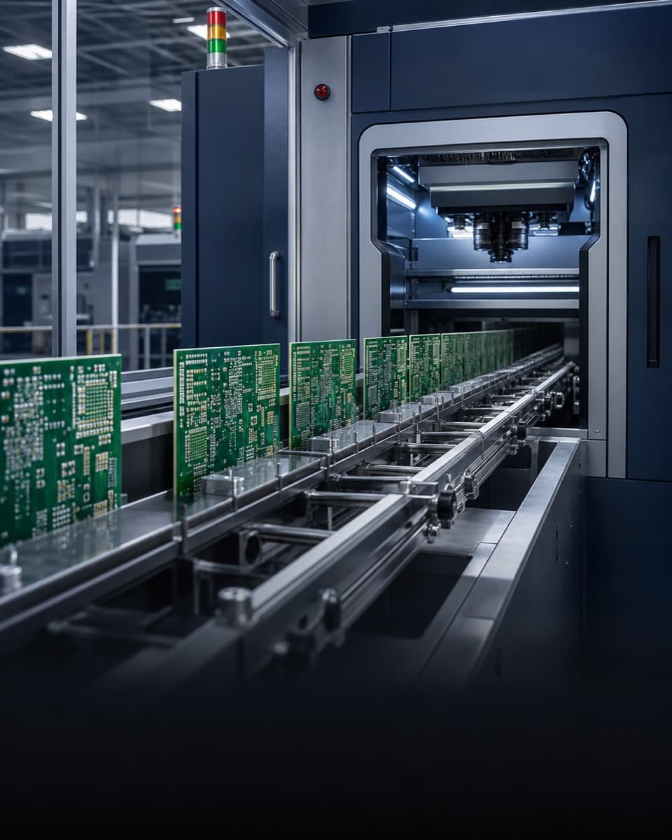
Volume production for rigid and multilayer PCB
| Layer count | 1–40 layers |
|---|---|
| Base materials | FR-4, High-Tg FR-4, halogen-free FR-4, Rogers, Taconic/AGC, PI, aluminum, PTFE/Teflon, F4B and other specialty laminates |
| Board thickness | 0.10–10.0 mm |
| Minimum trace / spacing | 2.5 / 2.5 mil (0.0625 / 0.0625 mm) |
| Minimum mechanical drill | 0.15 mm |
| Minimum laser via | 0.10 mm |
| Standard aspect ratio | Up to 15:1 |
| Copper thickness | 0.5–12 oz, depending on board type and construction |
| Controlled impedance | ±10% standard; ±5% for tighter requirements |
| Warpage | ≤0.75% standard; ≤0.5% available when specified |
| Surface finishes | HASL, Lead-Free HASL, OSP, ENIG, Immersion Silver, Immersion Tin, ENEPIG, Hard Gold, Gold Finger and selective finishes |
R&D prototype and high-end HDI builds
| Layer count | Up to 64 layers for prototype / engineering builds |
|---|---|
| Minimum trace / spacing | 2 / 2 mil (0.05 / 0.05 mm) |
| Standard mechanical drill | 0.15 mm |
| Advanced / special hole capability | Down to 0.10 mm, subject to design and process review |
| Minimum laser microvia | 0.075 mm |
| Aspect ratio | Up to 20:1 for qualified designs; 15:1 or below for standard advanced production |
| HDI structures | 1+N+1, 2+N+2, multi-step HDI and Any-Layer HDI |
| Via technology | Blind vias, buried vias, stacked vias, staggered vias, via-in-pad, VIPPO / POFV, resin-filled and plated-over vias |
| Sequential lamination | Supported |
| Any-layer interconnection | Supported |
| Back drilling | Supported |
| Controlled impedance | ±10% standard; ±5% for tighter requirements |
| Warpage control | ≤0.5% available when specified, subject to stack-up and design review |
| High-speed / high-frequency materials | Rogers, Taconic/AGC, PTFE/Teflon, F4B, High-Tg FR-4 and other low-loss specialty laminates |
Flexible constructions and mechanical qualification
| Layer count | 1–12 layers |
|---|---|
| Flexible materials | PI (Kapton), PET, LCP; High-Tg FR-4 in rigid areas |
| Flexible area thickness | 0.1–0.6 mm |
| Rigid-flex overall thickness | Up to 3.2 mm |
| Copper weight | 1/3–2 oz |
| Minimum trace / spacing | 3 / 3 mil standard; 2 / 2 mil advanced |
| Dynamic flexing | Defined by bend radius, copper, stackup and qualification plan |
| Supported features | Coverlay, stiffeners, ZIF contacts, shielding layers, SMT |
| Testing | Electrical, AOI, dynamic flex and custom testing as specified |
Business-day planning ranges after file and process review
| Product Type | Prototype (1–10 sqm) | Small Batch (10–50 sqm) | Mass Production (>50 sqm) |
|---|---|---|---|
| Double-Sided (2L) | 24–48 Hours | 3–5 Business Days | 7–9 Business Days |
| Multilayer (4–6L) | 48–72 Hours | 4–6 Business Days | 8–10 Business Days |
| Multilayer (8–12L) | 4–6 Business Days | 7–10 Business Days | 10–15 Business Days |
| Multilayer (12–18L) | 6–8 Business Days | 10–12 Business Days | 12–18 Business Days |
| Multilayer (18L+) | 7–12 Business Days | 12–15 Business Days | 15–20 Business Days |
| HDI PCB | 7–12 Business Days | 12–15 Business Days | 15–20 Business Days |
| Flexible PCB | 4–5 Business Days | 6–8 Business Days | 10–14 Business Days |
| Rigid-Flex | 7–10 Business Days | 10–14 Business Days | 15–20 Business Days |
Capability values are design-dependent. Material, copper weight, layer count, via structure, finished thickness and surface finish can change the achievable combination.
Material selection changes achievable geometry, impedance behavior and thermal performance. Confirm the laminate and special processes before the layout is frozen.
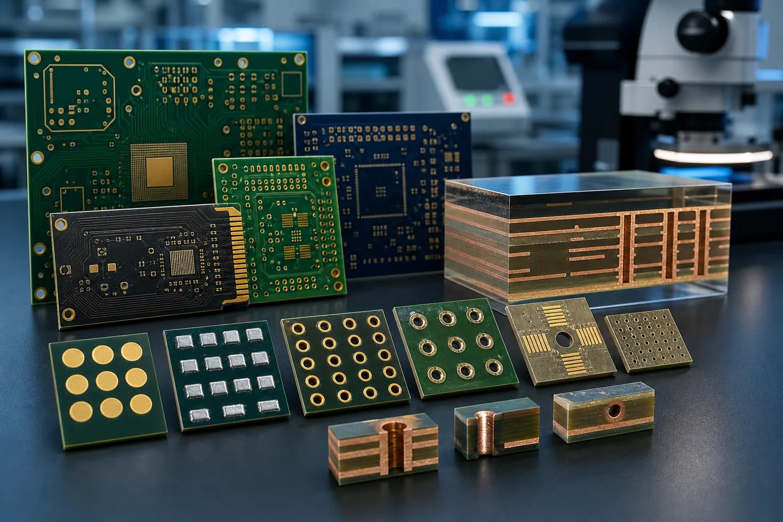
Match the board type to its qualified process window, then review the combined stackup, drill, copper, finish and testing requirements.
Use these examples as a starting point. The board construction still follows the product’s electrical, mechanical and qualification requirements.
PCB fabrication and PCBA operations are coordinated across qualified manufacturing locations. The applicable production site is confirmed during quotation.
Gerber, materials, stackup, geometry, via structure and testing requirements reviewed before tooling.
Single-board prototype, small batch and volume production paths.
IPC-A-600 and IPC-A-610 acceptance criteria applied as specified by the drawing.
Quality-system and compliance documentation is available for applicable manufacturing operations. Request the current certificates and scope during supplier qualification.
Confidential file handling and NDA availability for design-data exchange.
Quality documents
The published ISO records name Zhongshan Wenquan Electronic Manufacturing Co., Ltd. and its Zhongshan PCBA facility. They do not certify every PCBArise facility, service or product.
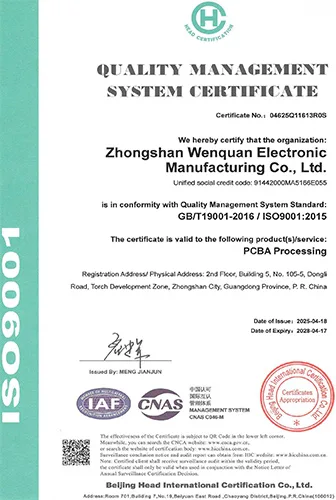
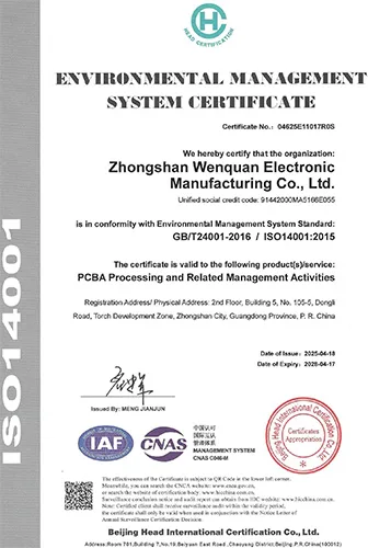
These are management-system certificates, not product or batch COAs. No batch inspection reports or COAs are currently published here.
These answers explain how to interpret published capability values and prepare a build for final confirmation.
Volume production supports 1–40 layers. Prototype and engineering builds can support up to 64 layers, subject to file-level review because geometry and lamination complexity become the governing limits.
Standard rigid production is 2.5/2.5 mil. Advanced builds can reach 2/2 mil, while flexible PCB is 3/3 mil standard with 2/2 mil available.
Standard production uses a 0.15 mm mechanical drill and 0.10 mm laser via. Advanced and special-hole capability reaches down to 0.10 mm, with minimum laser microvias of 0.075 mm.
Use them for early design screening, then submit the complete stackup and fabrication package. Final capability depends on the combination of material, copper, geometry, drilling and finish.
Move from the capability reference to a board technology, DFM review or prototype build.
Share the available Gerber, ODB++, drawing, stackup or project requirements with the PCBArise team.