
4–6 layers
A routing pair plus dedicated power and ground planes for mainstream products.
Need more room for routing, stable return paths or separate power planes? Multilayer PCB manufacturing gives your design a stackup built around those needs. PCBArise reviews whether 4, 6 or more layers make sense for the actual signals, components and board size.
Board size alone does not set the layer count. Plane count, escape routing, signal integrity and lamination cycles are the decisions that matter.
A routing pair plus dedicated power and ground planes for mainstream products.
Multiple reference planes for DDR, PCIe and mixed-signal architectures.
Backplanes, line cards and complex analog/digital partitioning.
High-count backplanes and instrumentation requiring careful lamination planning.
Standard production covers most multilayer designs. High-count, HDI or unusually tight geometries move into an advanced review path.
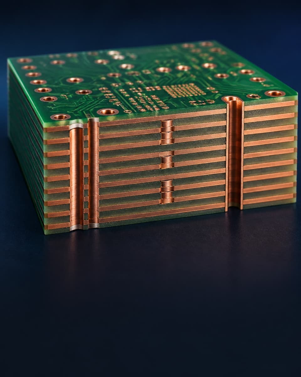
The baseline volume production window
| Layer count | 1–40 layers |
|---|---|
| Base materials | FR-4, High-Tg FR-4, halogen-free FR-4, Rogers, Taconic/AGC, PI, aluminum, PTFE/Teflon, F4B and other specialty laminates |
| Board thickness | 0.10–10.0 mm |
| Minimum trace / spacing | 2.5 / 2.5 mil (0.0625 / 0.0625 mm) |
| Minimum mechanical drill | 0.15 mm |
| Minimum laser via | 0.10 mm |
| Standard aspect ratio | Up to 15:1 |
| Copper thickness | 0.5–12 oz, depending on board type and construction |
| Controlled impedance | ±10% standard; ±5% for tighter requirements |
| Warpage | ≤0.75% standard; ≤0.5% available when specified |
| Surface finishes | HASL, Lead-Free HASL, OSP, ENIG, Immersion Silver, Immersion Tin, ENEPIG, Hard Gold, Gold Finger and selective finishes |
R&D prototyping and high-end builds
| Layer count | Up to 64 layers for prototype / engineering builds |
|---|---|
| Minimum trace / spacing | 2 / 2 mil (0.05 / 0.05 mm) |
| Standard mechanical drill | 0.15 mm |
| Advanced / special hole capability | Down to 0.10 mm, subject to design and process review |
| Minimum laser microvia | 0.075 mm |
| Aspect ratio | Up to 20:1 for qualified designs; 15:1 or below for standard advanced production |
| HDI structures | 1+N+1, 2+N+2, multi-step HDI and Any-Layer HDI |
| Via technology | Blind vias, buried vias, stacked vias, staggered vias, via-in-pad, VIPPO / POFV, resin-filled and plated-over vias |
| Sequential lamination | Supported |
| Any-layer interconnection | Supported |
| Back drilling | Supported |
| Controlled impedance | ±10% standard; ±5% for tighter requirements |
| Warpage control | ≤0.5% available when specified, subject to stack-up and design review |
| High-speed / high-frequency materials | Rogers, Taconic/AGC, PTFE/Teflon, F4B, High-Tg FR-4 and other low-loss specialty laminates |
Capability values are design-dependent. Material, copper weight, layer count, via structure, finished thickness and surface finish can change the achievable combination.
Every sequential lamination cycle adds process steps. The engineering goal is to preserve routing density while removing avoidable via complexity.
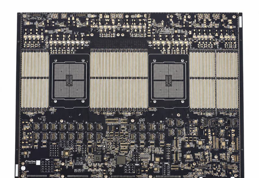
Review layer symmetry, copper balance, via architecture, impedance references and lamination cycles as one multilayer build system.
Use these examples as a starting point. The board construction still follows the product’s electrical, mechanical and qualification requirements.
Line cards and backplanes with controlled return paths.
Mixed analog, digital and power sections in one board.
DDR, PCIe and SerDes routing with defined impedance.
Dense control, sensing and ADAS-related electronics.
Monitoring and diagnostic systems with routing-density constraints.
Backplanes, power management and high-connector-count designs.
Quality documents
The published ISO records name Zhongshan Wenquan Electronic Manufacturing Co., Ltd. and its Zhongshan PCBA facility. They do not certify every PCBArise facility, service or product.


These are management-system certificates, not product or batch COAs. No batch inspection reports or COAs are currently published here.
These answers cover the stackup, via and impedance questions that commonly affect multilayer PCB release.
The standard volume production range is 4–40 layers. Prototype and engineering stackups can support up to 64 layers and require a separate engineering evaluation.
Yes. Blind, buried, stacked and staggered microvia structures are available. The lamination sequence is reviewed because it drives both reliability and cost.
Yes. Send the netlist, target impedance and material constraints. Engineering can propose the lowest practical layer count and a manufacturable stackup.
Standard multilayer production targets ±10%. ±5% is available for tighter requirements after the full stackup and material system are confirmed.
Continue to HDI, rigid PCB, manufacturing capabilities or DFM review according to the routing constraint.
Share the available Gerber, ODB++, drawing, stackup or project requirements with the PCBArise team.