
Oscilloscopes, spectrum analyzers, signal generators and electronic loads
Industries / PCB & PCBA
Test & Measurement PCB Manufacturer
PCBArise manufactures test and measurement PCB/PCBA for oscilloscopes, data-acquisition systems, electronic test fixtures, laboratory instruments, calibration equipment and industrial measurement products. The board is qualified against the instrument’s signal chain—low-noise analog, sampling, timing, shielding, connector, calibration and test access—rather than against a generic assembly checklist.
Low-Noise ReviewControlled ImpedanceTest Access PlanningTraceable Build Records
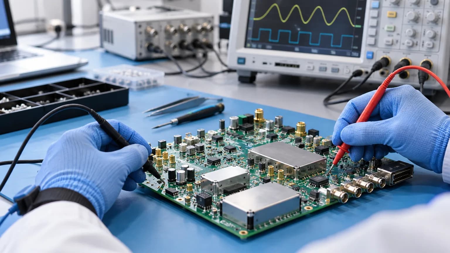
Product useOscilloscope, DAQ & Instrumentation PCB ApplicationsChosen for your product
Board constructionPrecision Instrument PCB Construction
Assembly routeInstrumentation PCBA for DAQ, Testers & Calibration Tools
Quality checksMeasurement PCB Inspection, Calibration & Test Evidence
Typical applications
Oscilloscope, DAQ & Instrumentation PCB Applications
Test-instrument buyers need a PCB supplier that understands what the board measures. We connect the PCB and PCBA route to the instrument type, signal path, fixture and calibration method.
Data-acquisition (DAQ), analog front-end and precision sensor boards
Laboratory power supplies, meters and calibration instruments
Automated test equipment, ICT/FCT fixtures and production testers
Industrial monitoring, condition-monitoring and control measurement units
High-speed interface, instrumentation backplane and embedded measurement boards
Engineering choices
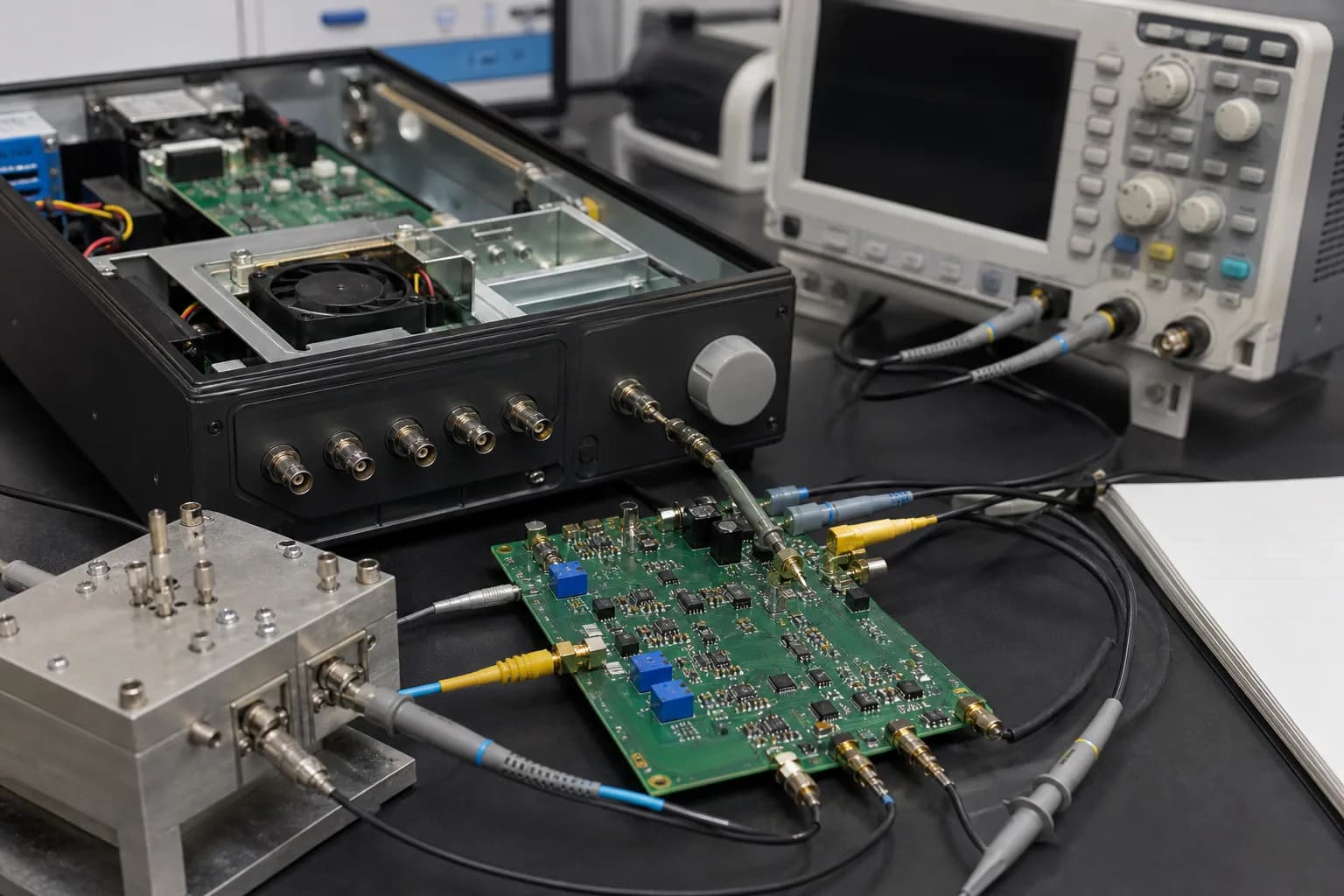
What Instrumentation PCB Buyers Need to Qualify
A measurement PCBA can pass continuity and still miss noise, drift, timing or calibration limits. The manufacturing plan therefore starts with the instrument’s measurement margin and acceptance method.
Low-noise analog and sensor channels need clean references, guarding, return paths and contamination control
High-speed sampling and clocks require impedance, length and layer geometry to remain stable
Thermal drift and self-heating affect gain, offset and calibration repeatability
Connectors, shielding, guarding and fixture interfaces must stay mechanically consistent
Test points, programming and calibration access belong in the instrument release, not as a late add-on
Prototype measurements and changes must be documented before production data is frozen
Board and process options
Precision Instrument PCB Construction
Standard multilayer, controlled-impedance, high-Tg and advanced HDI constructions are selected against the oscilloscope, DAQ, fixture or calibration instrument’s signal and mechanical requirements.
Product focus
Precision instruments expose manufacturing variation quickly.
Low-noise analog paths, high-speed sampling, calibration and fixture interfaces need to remain stable from prototype learning through repeat production.
- Low-noise and guarding strategy
- Test points and calibration access
- Functional limits and documented records
Precision Instrument Signal-Path PCB Review
Construction values assessed against noise, impedance, drift, shielding and connector behavior
| Parameter | Specification |
|---|---|
| Base Material | FR-4, High-Tg FR-4, halogen-free FR-4, Rogers, Taconic/AGC, PI, aluminum, PTFE/Teflon, F4B and other specialty laminates |
| Min Trace Width / Spacing | 2.5 / 2.5 mil (0.0625 / 0.0625 mm) |
| Min Mechanical Drill | 0.15 mm |
| Controlled Impedance | ±10% standard; ±5% for tighter requirements |
| Warpage | ≤0.75% standard; ≤0.5% available when specified |
| Surface Finishes | HASL, Lead-Free HASL, OSP, ENIG, Immersion Silver, Immersion Tin, ENEPIG, Hard Gold, Gold Finger and selective finishes |
Board and process options
DAQ, Oscilloscope & Low-Noise Analog Options
Dense instrument boards may combine fine-pitch processors, analog front ends, high-speed interfaces and shielding. Advanced stackup and via choices are confirmed against the actual measurement path and fixture.
Product focus
Precision instruments expose manufacturing variation quickly.
Low-noise analog paths, high-speed sampling, calibration and fixture interfaces need to remain stable from prototype learning through repeat production.
- Low-noise and guarding strategy
- Test points and calibration access
- Functional limits and documented records
DAQ & High-Speed Measurement Interconnect Review
Advanced options selected around sampling, timing, channel isolation and fixture access
| Parameter | Specification |
|---|---|
| Min Trace Width / Spacing | 2 / 2 mil (0.05 / 0.05 mm) |
| Controlled Impedance | ±10% standard; ±5% for tighter requirements |
| Back Drilling | Supported |
| Warpage Control | ≤0.5% available when specified, subject to stack-up and design review |
| High-Speed / High-Frequency Materials | Rogers, Taconic/AGC, PTFE/Teflon, F4B, High-Tg FR-4 and other low-loss specialty laminates |
| Board Thickness Tolerance | ±0.05 mm |
Assembly considerations
Materials for Precision Measurement & Test Fixtures
Material and finish decisions follow signal integrity, thermal drift, solderability, connector durability, cleanliness, fixture wear and lifecycle requirements.
Options to discuss
Start with what your design needs.
We can confirm the workable combination after reviewing your files.
FR-4High-Tg TG170RogersTaconicPIAluminumENIGENEPIGImmersion SilverOSPHard GoldShielding
What to send
Choose for the product you are building.
- Low-noise and guarding strategy
- Test points and calibration access
- Functional limits and documented records
Board and process options
Instrumentation PCBA for DAQ, Testers & Calibration Tools
Fine-pitch ICs, precision passives, connectors, shields, sensors and mixed-technology content are assembled to the approved BOM, stencil, workmanship class and instrument test procedure.
Product focus
Precision instruments expose manufacturing variation quickly.
Low-noise analog paths, high-speed sampling, calibration and fixture interfaces need to remain stable from prototype learning through repeat production.
- Low-noise and guarding strategy
- Test points and calibration access
- Functional limits and documented records
Instrumentation Assembly & Fixture Interface Window
Placement and process values reviewed with precision components, shielding and calibration access
| Parameter | Specification |
|---|---|
| Min Component Size | 01005 (0.4 × 0.2 mm) |
| Min QFP / QFN Pitch | 0.15 mm spacing / 0.3 mm width |
| Placement Accuracy (X/Y) | ±0.025 mm (±25 μm) |
| Placement Accuracy (θ) | ±0.2° |
| Warpage Control | ≤0.5%(Subject to board construction and assembly process review) |
| Soldering Methods | Wave Soldering, Selective Soldering, Hand Soldering |
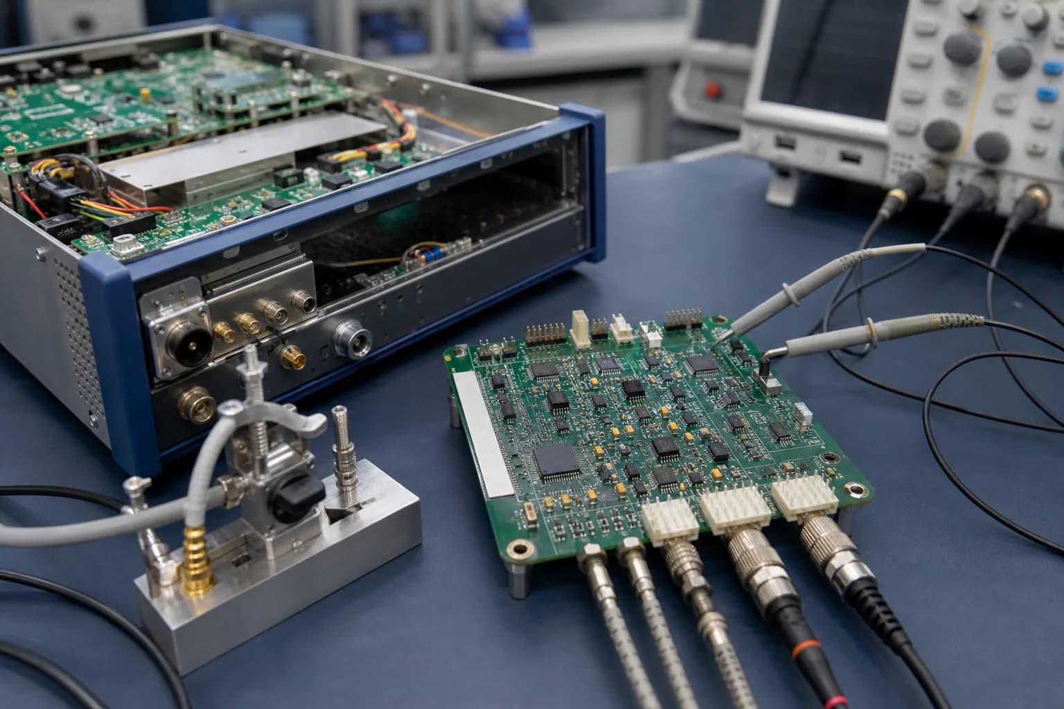
How the board fits the product
Precision instruments expose manufacturing variation quickly.
Low-noise analog paths, high-speed sampling, calibration and fixture interfaces need to remain stable from prototype learning through repeat production.
- Low-noise and guarding strategy
- Test points and calibration access
- Functional limits and documented records
Low-Noise ReviewControlled ImpedanceTest Access PlanningTraceable Build Records
Inspection, testing and records
Measurement PCB Inspection, Calibration & Test Evidence
SPI, AOI, X-ray, ICT, flying probe, functional fixtures, programming, calibration support and final inspection are selected according to the oscilloscope, DAQ, tester or instrument acceptance plan. Records are defined by the project rather than assumed from a generic capability list.
ISO 9001:2015ISO 14001:2015ICTFCTFlying ProbeCalibration Support
Build files
Keep the board revision, BOM and assembly drawings together so the factory builds the intended configuration.
Inspection and test
Choose optical, X-ray, electrical or functional checks for the defects that matter to this product.
Material tracking
Agree which material and production records you need to retrieve after shipment.
Design changes
Decide who can approve a material, component or process change before it reaches the line.
Quality documents
Preview & download certificates
The published ISO records name Zhongshan Wenquan Electronic Manufacturing Co., Ltd. and its Zhongshan PCBA facility. They do not certify every PCBArise facility, service or product.
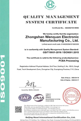
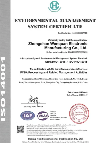
These are management-system certificates, not product or batch COAs. No batch inspection reports or COAs are currently published here.
Frequently asked questions
Common questions about this PCB application
Start with the board, environment and files you have; the detailed route depends on your design.
Can you build PCBs for oscilloscopes and electronic test instruments?
Yes. Typical work includes oscilloscopes, signal and power instruments, data acquisition, test fixtures, calibration equipment, and industrial measurement boards. Send the signal, mechanical, test-access, and acceptance requirements for an engineering review.
How do you control low-noise analog measurement boards?
We review stackup, ground and guard strategy, isolation, component placement, cleanliness, shielding, thermal paths, and the required electrical or functional test. The final controls follow the released design and measurement acceptance plan.
Can you manufacture controlled-impedance and high-speed measurement boards?
Yes. Stackup, differential impedance, trace geometry, length matching, back drilling, material, and production tolerance are reviewed against the interface and frequency requirements. Exact limits are confirmed for the released design.
What testing can be included for a measurement PCBA?
Depending on the project, testing may include SPI, AOI, X-ray, flying probe, ICT, FCT, programming, calibration steps, functional fixtures, and final inspection. Test points, procedures, limits, and records should be supplied with the RFQ.
Can you build prototypes and production units with the same process?
The review is designed to identify a production-relevant construction, assembly, and test route early. Once approved, the released data, materials, process controls, and acceptance records can be carried into production.
What should I include in a test-instrument PCB RFQ?
Include Gerber or ODB++ files, BOM, pick-and-place, schematics or block diagrams where useful, stackup and impedance targets, test points, fixture or calibration requirements, mechanical drawings, and the required inspection and acceptance records.
Related PCB pages
Explore the board and assembly options behind this product.
Use the related PCB, PCBA and quality pages to plan the next part of your build.
PCBArise resource
High Frequency PCB
RF materials and controlled-impedance construction.
PCBArise resourcePCB Materials & Stackup
Stackup, material, and signal-integrity review.
PCBArise resourcePCB Assembly Testing
Assembly inspection, electrical test, and functional validation.
PCBArise resourceDFM Review
Review test access and manufacturability before release.
PCBArise resourceQuality Control
Inspection, calibration, and documented production controls.
Protect the measurement margin in the manufacturing plan.
Share the signal, calibration, fixture, test-access and acceptance requirements with the engineering team.