
Pad, mask and via strategy
Confirm package drawing, pad geometry, solder-mask definition, via-in-pad treatment and escape construction before stencil decisions are frozen.
BGA assembly connects pad design, stencil strategy, placement, reflow and hidden-joint inspection in one build-specific process route. PCBArise reviews the released package before confirming how a BGA or fine-pitch assembly should be produced and accepted.
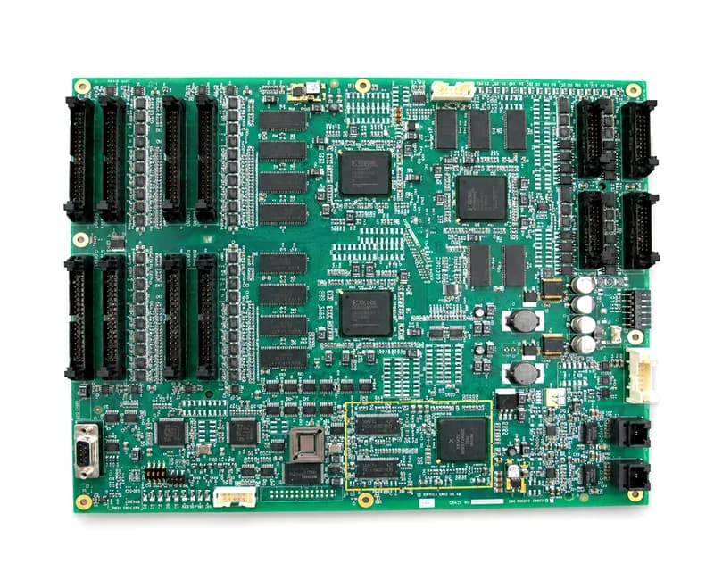
A ball grid array places its solder connections beneath the package, where ordinary visual inspection cannot confirm every joint. The assembly route therefore starts before placement: land pattern, via strategy, stencil aperture, paste volume, board support, package handling, reflow profile and inspection access need to describe one manufacturable design. The published PCBArise capability reference includes BGA, QFN and fine-pitch assembly together with 2D/3D AXI. These values are useful for initial supplier screening, but they are not blanket promises for every board. The released Gerber or ODB++, BOM, CPL, drawings, package data and acceptance requirements determine final process fit.
BGA risk is distributed across design, materials, equipment setup and evidence. Reviewing only the placement machine specification leaves the most important interfaces unresolved.
Confirm package drawing, pad geometry, solder-mask definition, via-in-pad treatment and escape construction before stencil decisions are frozen.
Select aperture form, stencil thickness, paste family and board support from package geometry and the surrounding component mix.
Align package handling, placement accuracy, board thermal mass, solder alloy and component temperature limits with the intended reflow route.
Use SPI, AOI, X-ray or electrical and functional evidence where each method can detect the defects defined for the build.
The following inputs turn a BGA request into an engineering review. Exact limits, equipment, facility, profile and inspection coverage are confirmed only after the production package is reviewed.
Final scope, limits and evidence are confirmed from the released build package.
| Required quote package | Gerber or ODB++, BOM, CPL/centroid data, assembly drawing, package information and available inspection or test requirements. |
|---|---|
| Package identity | Manufacturer part number, body size, ball map, pitch, moisture sensitivity and handling instructions where applicable. |
| Published pitch reference | 0.25 mm minimum BGA pitch is a published screening value; final fit depends on land pattern, board construction, stencil, process line and inspection plan. |
| Land-pattern review | Pad dimensions, solder-mask definition, paste layer, via-in-pad construction and component keep-out checked against the selected package. |
| Print strategy | Stencil thickness, aperture design, step requirements, paste type and board support reviewed with the complete package mix. |
| Placement data | Reference designator, X/Y origin, rotation, polarity conventions and package-library consistency resolved before programming. |
| Reflow route | Profile established from solder alloy, board thermal mass, finish, package limits and the rest of the component population. |
| Inspection route | SPI for paste, AOI for visible conditions and 2D/3D AXI for hidden-joint evidence where the approved plan requires it. |
| Rework decision | Access, adjacent components, board construction, thermal exposure and acceptance criteria reviewed before any rework route is authorized. |
| Test interface | ICT, flying probe, programming or functional test added when test access, fixture data, procedures and limits are available. |
Fine Pitch remains a section of the SMT and BGA service routes rather than a separate URL.
| Fine-pitch definition | Treat pitch as one input alongside pad geometry, lead or ball style, paste-release area ratio, board flatness and inspection access. |
|---|---|
| Neighbouring packages | Review tall, heat-sensitive or shielded components that can constrain placement, profiling, inspection or rework access. |
| Board support | Confirm panel rails, tooling holes, fiducials and underside clearance so printing and placement do not distort the board. |
| First-build evidence | Use first-article inspection and the approved evidence plan to close orientation, paste, profile and hidden-joint questions. |
| Change control | Recheck the route when package source, PCB finish, solder paste, stencil, panelization or board revision changes. |
| Acceptance boundary | Define which conditions are screened visually, by X-ray, electrically or functionally instead of assuming one method proves every joint. |
A correct footprint can still fail at launch if the BOM names a different package, the paste layer was not updated, the centroid rotation is wrong or the panel cannot be supported. The engineering review reconciles those interfaces and records which evidence will be returned. For broader placement and reflow context, use the existing SMT Assembly page; for published screening limits, use PCB Assembly Capabilities.
The review turns hidden-joint risk into explicit design, process and acceptance decisions before material is committed.
Use this route when hidden interconnects, dense package geometry or inspection evidence materially affect build readiness.
Close footprint, orientation, stencil, profile and inspection questions before the design moves into repeat production.
Coordinate processors, memory, power packages and surrounding fine-pitch parts within one print and reflow strategy.
Review shielding, thermal mass, high-density packages and inspection access without separating assembly from board construction.
Define project-specific component identity, process evidence and change control for the released assembly package.
Sequence BGA reflow with through-hole, press-fit and secondary soldering operations that follow it.
Connect hidden-joint evidence to the broader electrical and functional test plan instead of treating X-ray as a complete product test.
These answers help prepare a BGA request without turning a published capability reference into an unconditional promise.
Provide Gerber or ODB++, BOM, CPL or centroid data, assembly drawings, package information and available inspection or test requirements. The files should identify the same design revision and package source.
No. The published pitch is an initial screening reference. Final feasibility also depends on pad and mask design, via treatment, stencil, paste, board support, thermal mass, package handling, assigned equipment and inspection access.
The plan can combine print evidence, visible inspection, 2D/3D X-ray and electrical or functional testing. Each method detects different conditions, so coverage and acceptance criteria are confirmed for the build rather than assumed.
No. Fine-pitch requirements are reviewed within SMT and BGA assembly because package geometry, stencil, placement, reflow and inspection decisions share the same process interfaces.
A rework route can be evaluated after package access, adjacent-component clearance, board construction, thermal exposure, replacement material and acceptance evidence are reviewed. The page does not promise that every assembly is safely reworkable.
Move from BGA-specific process questions to mixed technology, inspection, prototype and capability decisions.
Share the current board data, BOM, CPL, drawings, package information and intended inspection or test evidence for an engineering-led quotation review.