
In short
Bare-board netlist testing checks the manufactured board’s electrical connections against a defined reference under specified test conditions. It can detect opens and unintended connections within that coverage, but it does not prove that the circuit design is correct, the assembled product works or every reliability risk is absent. Supply a current design-derived netlist where available, reconcile it with fabrication data and specify the result information you need.
- Keep design-derived connectivity separate from connectivity extracted from production artwork.
- A CAD-to-CAM comparison is a data check; electrical probing is a check on a physical board.
- Define test conditions, access exceptions, coverage and result identity before interpreting “pass”.
- Use separate requirements for impedance, insulation stress, workmanship, assembly and product function.
A bare-board electrical-test pass is a statement about specified connections on a particular board, not a blanket guarantee that the product will work. To use that statement well, identify the reference netlist, the physical units covered, the test conditions and any exceptions. Without those details, “electrically tested” can mean less than the buyer expects.
What does a netlist describe?
A netlist describes which electrical nodes belong together and which belong to different networks. For a bare PCB, the question is connectivity between conductive features before components are fitted. A design-derived netlist exported from the current PCB database can provide an independent reference against which manufacturing data is compared.
Keep that export synchronized with the final layout. Run the design tool's schematic-to-layout checks separately: an export from an incorrectly routed or outdated PCB database is not proof of the intended circuit. The familiar term IPC-D-356 identifies an exchange format, not a guarantee that a particular file is correct, complete or accepted by every system. Other supported intelligent data can carry connectivity; establish what the actual import uses.
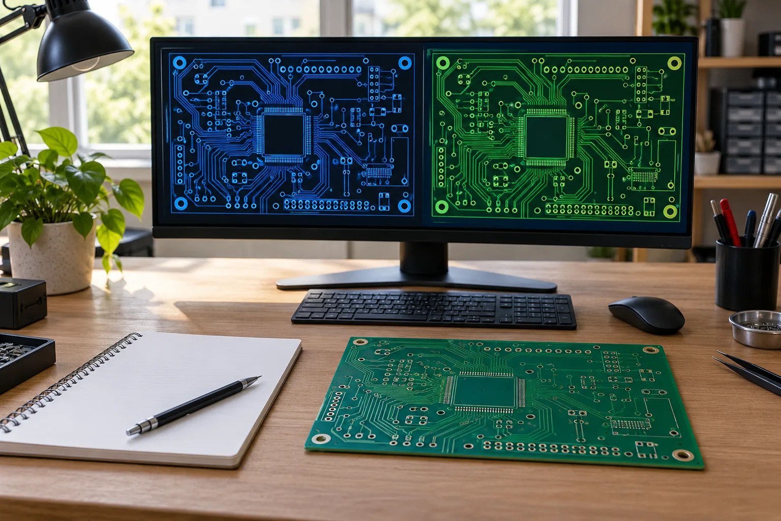
Conceptual design-to-CAM comparison; not an exported customer netlist or a validated software report.
Why is a design-derived netlist different from a CAM-extracted netlist?
They come from different representations of the board. The design reference comes from the design database; a CAM extraction infers connectivity from the artwork and drilling representation being prepared for production. Comparing the two can expose a connectivity mismatch before boards are made.
| Check | Compared objects | Useful conclusion | Important limit |
|---|---|---|---|
| Design connectivity review | Schematic intent and current PCB database. | The design representations agree within the review performed. | A consistently wrong design can still be wrong. |
| CAD-to-CAM netlist comparison | Design reference and connectivity extracted from fabrication data. | Data translation or preparation differences can be found. | No physical board has been tested by this comparison. |
| Bare-board electrical test | Physical board measurements and the selected reference/test program. | Covered connections meet the stated test criteria. | Untested properties and product function remain outside the conclusion. |
Testing only against a netlist extracted from the same erroneous artwork may reproduce that artwork's unintended connection as the expected condition. An independent design reference helps detect that mismatch; it does not remove the need to review the design itself. Eurocircuits describes both artwork-derived production connectivity and the value of including a CAD-exported reference. That is a useful distinction, not evidence that every supplier uses an identical workflow.
What do continuity and isolation tests actually check?
Continuity checks expected connections; isolation checks separation between networks that should not be connected, under the defined electrical conditions. An open interrupts an intended path. A short joins paths that should be separate. Test limits, voltage, contact strategy and coverage determine which conditions can be detected.
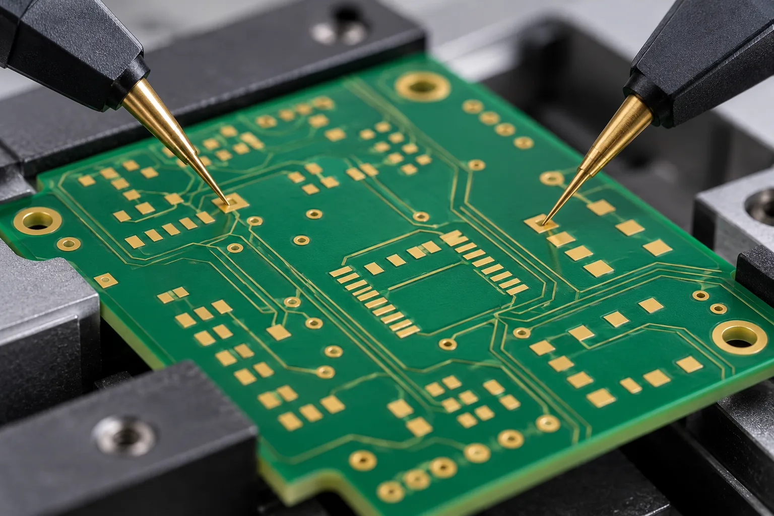
Conceptual probe contact only; pad access, test settings and actual readings must come from the real test plan.
Do not insert a universal resistance or voltage into a purchase note merely because another article lists one. State the applicable specification and revision, required test conditions and any design-specific constraints. If high-voltage insulation, dielectric withstand or another stress test is required, specify it separately with its qualified method and limits. A routine connectivity pass must not be relabeled as safety qualification.
Likewise, controlled-impedance verification addresses a different property from DC connectivity. A connected trace can still have the wrong impedance. Physical inspection, dimensional checks, material verification and reliability testing answer other questions. The buyer should combine the necessary checks, not ask one electrical pass to stand in for all of them.
Does flying probe or a fixture change what “pass” means?
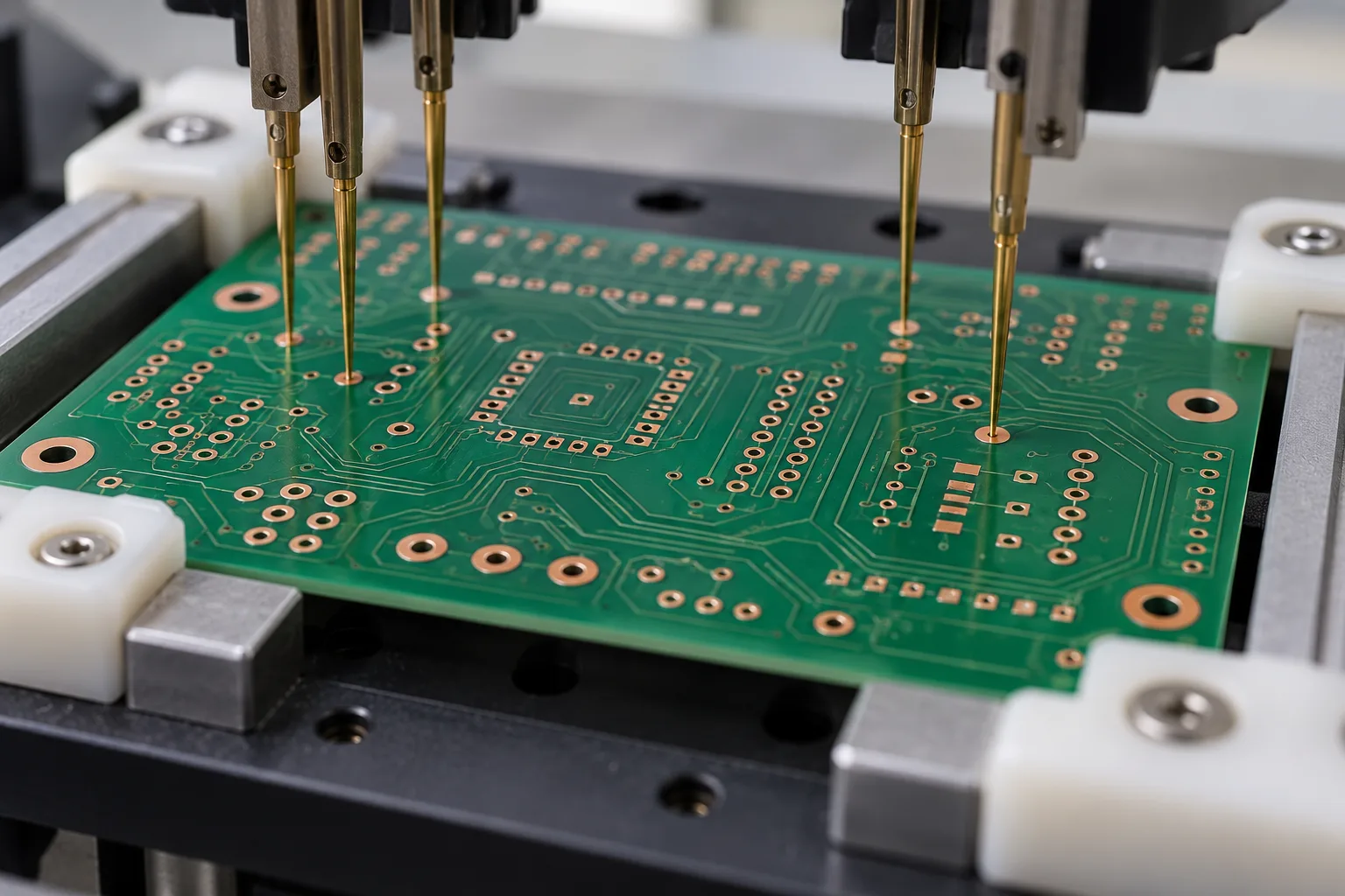
The method changes access, preparation and throughput; the meaning of a pass still depends on the reference, coverage and limits. Moving probes can reach selected exposed features without a dedicated full-board fixture. A fixture makes repeated contact through a designed pin arrangement. Neither method automatically establishes that every requested network, board or special structure was covered.
| Planning question | Moving-probe route | Fixture route |
|---|---|---|
| Preparation | Validated program and accessible contact locations. | Validated program plus board-specific contact tooling. |
| Design change | Recheck data, access and program after the change. | Also recheck whether the tooling still matches. |
| Coverage | Document contacted features and exclusions. | Document pin access, fixture condition and exclusions. |
| Buying decision | Compare the actual quantity, access and test time. | Compare tooling effort and repeat-run needs. |
These are planning differences, not a price promise or a claim about PCBArise equipment. Populated-board ICT and functional tests require different inputs and interpretation; use the separate PCBA test-method guide for that task. A bare board contains no fitted components or firmware whose operation could be proven by this pass.
How should a mismatch, failed contact or failed board be handled?
Keep data mismatch, contact uncertainty and a confirmed electrical defect as separate findings. A CAD-to-CAM difference first needs a design/data decision. A doubtful probe contact needs examination of access, contact and the test setup. A confirmed defect needs a recorded disposition and any retest specified by the governing requirements.
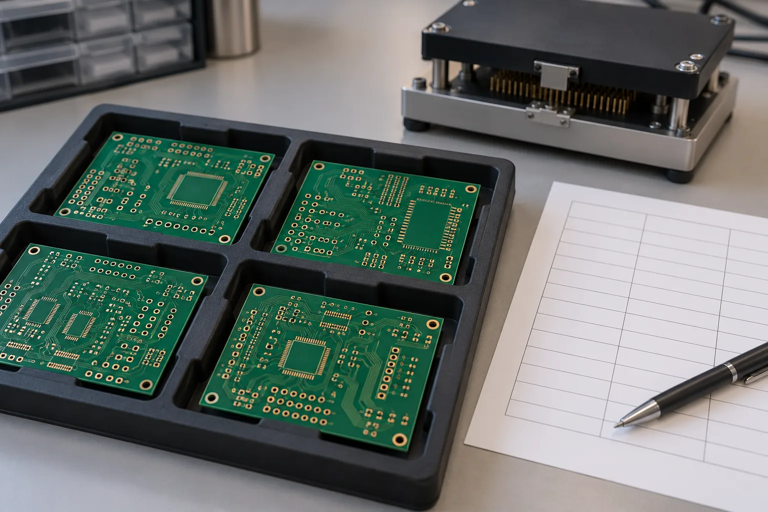
Conceptual test-result handoff; no actual pass, failed board, repair or shipment record is depicted.
A retest should not silently erase the first failure. Link the original result, investigation, permitted repair if any, changed setup and final result to the same unit or lot identity. If individual serial identity is not part of the order, define the available lot/panel/unit mapping honestly instead of promising a record the process cannot produce.
What should the buyer put in the test brief and result request?
Ask for enough information to connect the test conclusion to the ordered board and the agreed coverage. The following blank template is a preparation aid, not an existing PCBArise report.
Bare-board test brief — blank template
PCB part/revision [ ] | Drawing/package ID [ ] | Design-reference file/version [ ] | Export source/date [ ] | CAM comparison result/reference [ ]
Test definition: Applicable specification/revision [ ] | Method/program version [ ] | Continuity criteria [ ] | Isolation criteria [ ] | Test conditions [ ] | Access exceptions [ ] | Required unit/lot coverage [ ]
Result request: Lot/panel/unit mapping [ ] | Quantity tested [ ] | Pass/fail/exception quantities [ ] | Failed network/location reference [ ] | Contact investigation [ ] | Disposition/repair reference [ ] | Retest linkage [ ] | Test date/responsible function [ ]
Separate checks: Impedance [ ] | Insulation/stress test [ ] | Dimensions/workmanship [ ] | Other qualification [ ]
Attach the reference and brief to the fabrication drawing package. Review the proposed PCB manufacturing route and quality-record requirements together. Agree which results are supplied with the order; do not infer a comprehensive data package from a generic “electrical test included” line.
About the author
PCBArise Electronics
PCBArise Electronics publishes this guide to help design and NPI teams prepare clearer manufacturing files. The requirements for any actual build are confirmed from its current design package.
FAQ
Common questions
Does a bare-board electrical-test pass prove the assembled product works?+
No. It supports the covered bare-board connectivity under the stated test conditions. Component correctness, solder joints, firmware, interfaces and product behavior require their own assembly and functional checks.
Why supply a design-derived netlist if Gerber files already exist?+
It gives a separate connectivity reference for comparison with the fabrication data. A reference extracted only from the same faulty artwork may reproduce its error. Export from the current design and separately check schematic-to-layout agreement.
Is an IPC-D-356 file proof that the circuit design is correct?+
No. It is a data exchange, not a design qualification. Its usefulness depends on the source database, revision, export and import. A consistent but incorrect design can still produce a consistent netlist.
Is netlist comparison the same as testing a manufactured board?+
No. Netlist comparison checks data representations. Bare-board electrical testing measures physical connections against the chosen reference and criteria. Record both separately if both are required.
Does continuity testing also verify controlled impedance or high-voltage safety?+
No. Connectivity, impedance and electrical insulation or stress behavior are different requirements. Define the necessary separate methods, conditions and acceptance criteria instead of extending a connectivity pass beyond its coverage.
What should happen to the first failure when a board later passes retest?+
Keep it linked to the investigation and final result. Record whether the cause was contact, setup, a data problem or a physical defect, and retain any permitted repair and retest references. A later pass should not silently delete the earlier finding.
Technical references
Sources used for this guide
These sources explain the standards, materials or process details discussed above. Check the current revision when applying them to a new design.