
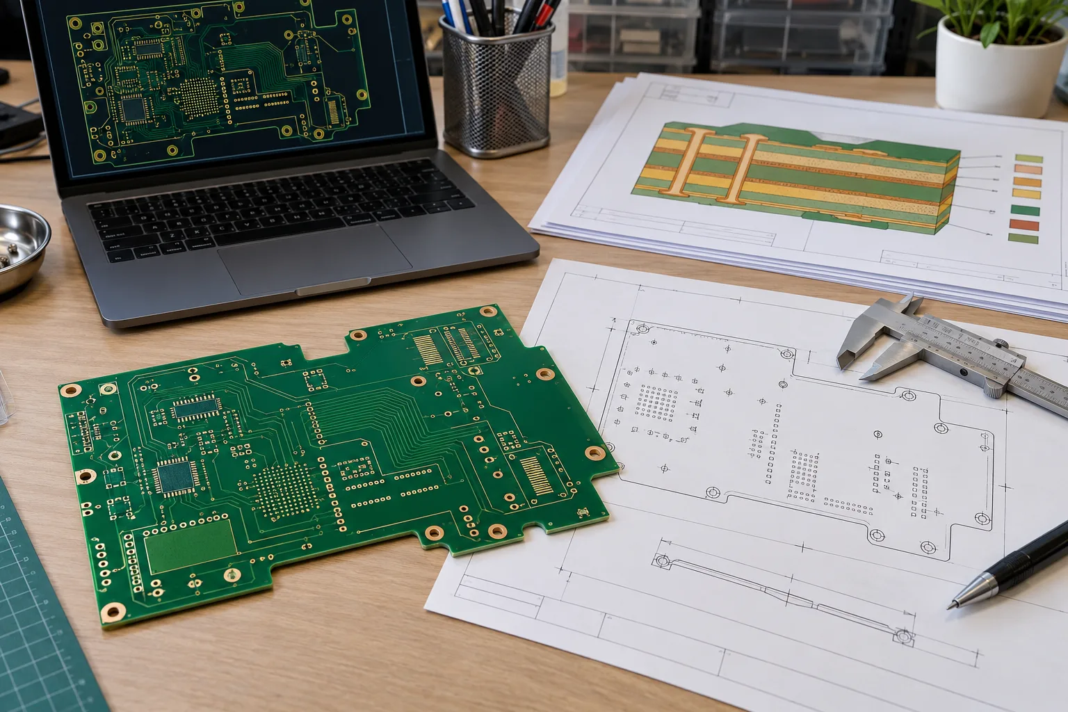
In short
A PCB fabrication drawing should define the finished bare board and agree with the files used to make it. Identify the board and revision, units, outline, finished holes, layer order, material, copper, finish and any special requirements. Cross-check each critical note against the actual data package; resolve contradictions before manufacturing rather than assuming that a drawing, purchase order or Gerber file always wins.
- Specify the finished feature the product needs, not an assumed machine setting or drill allowance.
- Keep one current drawing and a matching manifest of layer, drill, stackup and electrical-reference files.
- Identify exceptions such as plated slots, edge connectors, via treatment and restricted marking locations explicitly.
- A template is a starting point: remove irrelevant inherited notes and resolve conflicting requirements before the build.
Use a PCB fabrication drawing to say what the finished bare board must be, then check that its notes agree with the manufacturing files. A polished PDF cannot rescue a drill file from another revision or a finish selected differently on the order. The useful checklist is not a long collection of standard notes: it is a short, complete description of this board, with a clear way to resolve discrepancies.
What belongs on a fabrication drawing rather than an assembly drawing?
Put bare-board construction and acceptance requirements on the fabrication drawing; put component placement and assembly instructions on the assembly drawing. They can share a part-number family, but the bare PCB and populated assembly may have different part numbers and revision levels. State that relationship instead of forcing every document to carry an identical revision label.
| Document or data | Main question it answers | What it cannot replace |
|---|---|---|
| Fabrication drawing | What physical bare board is required? | Actual layer artwork and machine-readable drill geometry. |
| Layer, drill and route data | Where are copper, openings, holes and profile features? | An explicit material, finish and acceptance specification. |
| Assembly drawing, BOM and placement data | Which components go where, with what orientation and instructions? | The bare-board construction definition. |
| Purchase order and agreed specification | What quantity, deliverables and commercial requirements were ordered? | Resolution of a contradictory drawing or data set. |
For file-format selection use the separate Gerber, ODB++ and IPC-2581 guide. Here the task is consistency, not choosing a format. Ucamco explains that Gerber can carry attributes and a separate Job file for fabrication characteristics; “the information is not on the picture” does not always mean it is absent from the electronic package.
Which identity and mechanical details should be checked first?
Start with board identity, units, finished outline, datum and finished holes. Match the drawing number and revision to the manifest, not merely the ZIP filename. State whether delivery is individual boards or a specified array, and whether dimensions describe the board or the delivery panel.
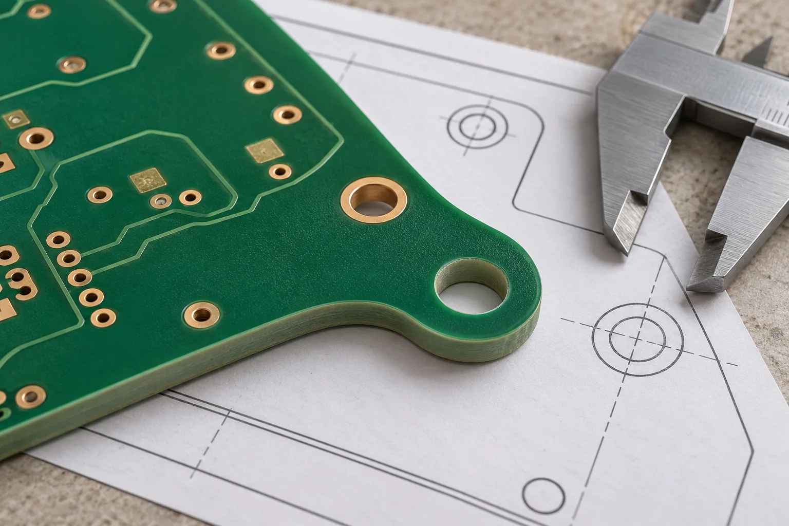
Conceptual outline and hole review; dimensions must come from the released design, not this image.
A complete mechanical definition covers external contour, cutouts, slots, critical hole locations, feature tolerances and reference surfaces. Make plated and non-plated features distinguishable. For a plated hole, state the required finished size after plating; do not add an undocumented drill oversize and hope that another fabricator uses the same allowance. A connector fit can fail even when an incorrectly specified hole was manufactured exactly as drawn.
Check that the NC drill and route files use the intended units, origin and orientation. Look at the imported output, not only the CAD source. A mounting-hole symbol, drill-table count and physical location should identify the same feature. If the drawing says a slot is plated but the route data labels it otherwise, log that specific feature and stop the affected operation until corrected data or a documented engineering decision resolves it.
How should stackup, copper and finish notes be made executable?
Describe the required construction and separate fixed product constraints from proposed manufacturing choices. List layer order and function, finished board thickness and tolerance, material requirements, copper requirements and surface finish. Where exact laminate or foil construction matters, identify it; where alternatives are permitted, state which properties and qualification requirements they must satisfy.
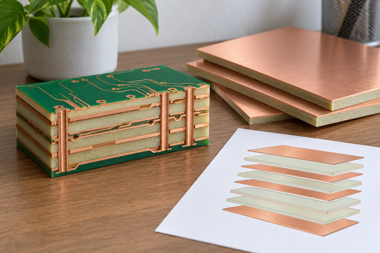
Conceptual stackup discussion; not a microsection, measured thickness or approved material construction.
Do not treat starting foil and finished copper as interchangeable. Identify which requirement applies to which layers. Likewise, a material's glass-transition temperature alone does not define continuous service temperature, all electrical properties or a product qualification. Link the actual material specification and keep any permitted substitution explicit.
Controlled impedance needs a defined structure, target, tolerance, reference layer and verification requirement; a note saying “controlled impedance” alone leaves the result undecidable. Keep detailed line geometry in the impedance handoff. Specify the selected finish rather than relying on a generic “lead-free” note when the exact finish matters. Solder mask and legend notes should distinguish material/process requirements from colour preferences and placement restrictions.
Which special features need their own notes?
Call out any feature whose intended result cannot be inferred reliably from ordinary artwork. Examples include filled and capped vias, blind/buried structures, plated edges, castellations, bevels, countersinks and restricted marking zones. Name the affected feature or layer span; a blanket via note can unintentionally change unrelated holes.
| Requirement | Record this | Common ambiguity to remove |
|---|---|---|
| Special hole or slot | Feature ID, finished geometry, plating status, location and tolerance. | Tool diameter mistaken for the finished opening. |
| Via treatment | Via group, fill/cap/tent requirement and applicable acceptance basis. | One note applied to every via regardless of function. |
| Markings | Required text or traceability content, side, location and exclusions. | Extra markings placed on a contact, keepout or mating surface. |
| Inspection and electrical test | Applicable document revision/class, source reference, checks and requested result format. | A generic “tested” note treated as complete product qualification. |
Do not copy a standard number, class or tolerance from another product without checking applicability. A class label does not replace the relevant specification and actual design requirements. This guide does not reproduce paid IPC clauses or prescribe universal hole, copper, insulation or acceptance limits.
What should happen when the drawing and data disagree?
Identify the conflict and obtain a single consistent manufacturing baseline before the affected work starts. Do not silently give precedence to whichever file looks newest. A purchase-order precedence rule can define how a conflict is escalated, but cannot make two incompatible physical requirements simultaneously achievable.
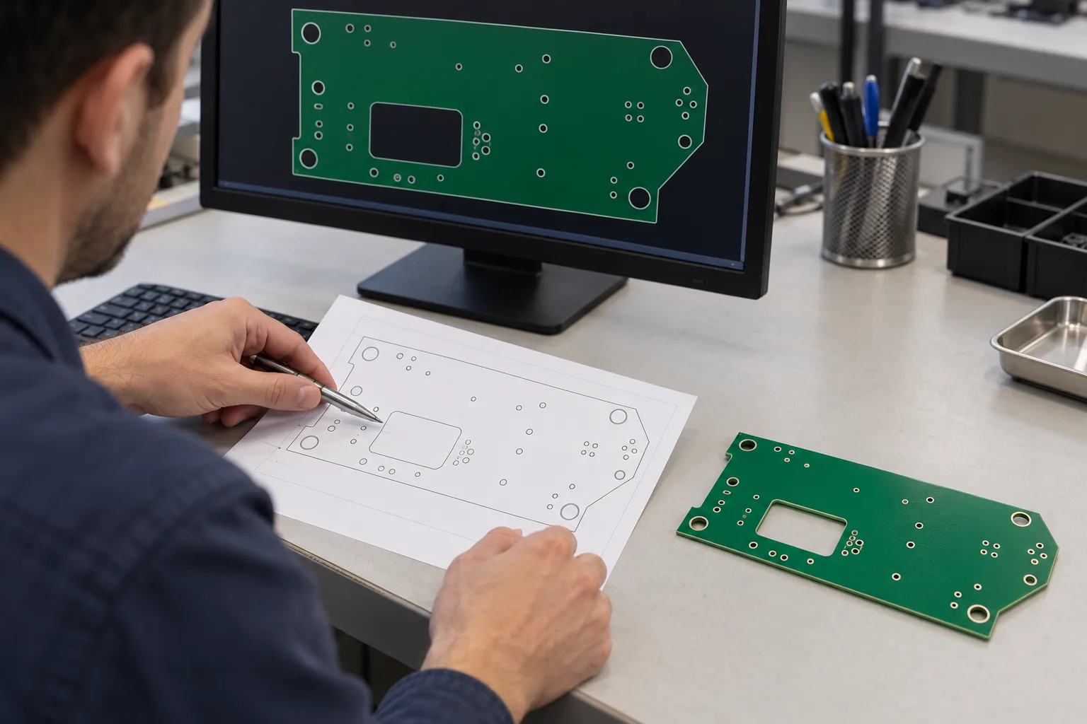
Conceptual file-to-drawing cross-check; no real engineering decision or customer documentation is shown.
For example, a hypothetical drawing asks for one finish while the order selects another. The correct action is to choose the required finish and update the contradictory input, not to let production decide by convention. The same logic applies to a changed thickness, missing slot plating or a netlist exported before the last layout edit. These are examples of decisions to make, not PCBArise production incidents.
Can this checklist be copied into a manufacturing handoff?
Yes. Fill the fields below and attach the matching files; leave no critical requirement hidden in an email thread. Mark irrelevant fields “not applicable” with a reason rather than keeping obsolete instructions.
Drawing checklist — blank template
Board part/revision [ ] | Assembly relationship [ ] | Drawing/revision [ ] | Units/datum [ ] | Individual board or delivery array [ ]
Geometry: Outline/cutout source [ ] | Critical dimensions/tolerances [ ] | Finished hole/slot sizes [ ] | Plated/non-plated identification [ ] | Drill/route file versions [ ]
Construction: Stackup source [ ] | Finished thickness/tolerance [ ] | Material specification/alternatives [ ] | Copper basis by layer [ ] | Finish [ ] | Mask/legend [ ] | Special features/marking exclusions [ ]
Acceptance: Applicable documents/revisions [ ] | Electrical reference [ ] | Inspection/test deliverables [ ] | Agreed exceptions [ ]
Consistency record: Conflicting file/note [ ] | Affected feature [ ] | Required correction/decision [ ] | Responsible person/date [ ] | Replacement package ID [ ]
Use the completed checklist with PCB DFM review or your bare-board manufacturing package. Include the drawing, layer/drill files, quantity and outstanding questions. It supports a precise review; it is not a claim that every listed inspection or special process is automatically included in a PCBArise order.
About the author
PCBArise Electronics
PCBArise Electronics publishes this guide to help design and NPI teams prepare clearer manufacturing files. The requirements for any actual build are confirmed from its current design package.
FAQ
Common questions
Is a fabrication drawing the same as a Gerber file?+
No. A fabrication drawing communicates finished-board requirements and references; Gerber layer data describes geometry and may also carry attributes. A Gerber Job file can carry additional fabrication characteristics. Check the complete package rather than assuming one file contains everything.
Should a plated hole be specified by drill size or finished size?+
Specify the finished hole size and tolerance required by the design, and identify it as plated. The fabricator selects the production tool and process allowance. Do not add an undocumented oversize that may conflict with that process.
Does every fabrication drawing need the same standard notes?+
No. Use a template only after checking each note against this board. Keep applicable material, geometry, construction and acceptance requirements; remove obsolete or irrelevant instructions. State the applicable document revisions rather than copying an unsupported class or limit.
Which file takes priority when the drawing and order conflict?+
Do not resolve a physical contradiction by assumption. Identify the affected requirement, apply the agreed escalation or precedence arrangement and obtain one consistent correction or engineering decision before the affected manufacturing work starts.
Can a PDF drawing replace drill and layer files?+
Normally it should accompany, not replace, the machine-readable fabrication data. Use the drawing to define requirements and cross-check imported geometry; provide the actual layer, drill and route files accepted for the manufacturing route.
Does this checklist define PCBArise inspection capability?+
No. It is a buyer preparation template. Specify the inspection and test results required for the particular build and align them with the proposed manufacturing route. A checklist field is not proof of equipment, qualification or an included service.
Technical references
Sources used for this guide
These sources explain the standards, materials or process details discussed above. Check the current revision when applying them to a new design.