
Quick answer
An RF stackup should begin with the operating band, transmission-line behavior, impedance and loss objectives—not a laminate brand alone. Compare supplier datasheet values using their stated test methods, then model the selected dielectric thickness, copper profile, trace and via geometry together. Ask the fabricator to review availability and achievable construction before releasing one controlled stackup revision.
An RF PCB material decision connects circuit behavior to a physical construction that a fabricator can repeatedly build. The laminate name matters, but so do the test method behind its datasheet values, copper profile, dielectric thickness, transmission-line geometry, reference planes, via transitions, finish and the tolerances carried into fabrication.
This guide owns the RF material and stackup selection workflow. The PCB Materials and Stackup page remains the commercial capability destination, while High Frequency PCB and Telecom RF PCB cover related manufacturing and application enquiries. Values and acceptance limits must come from the selected material data, design model and approved project package.
Direct answer: how do you choose an RF PCB material and stackup?
Define the operating band, interconnect length, transmission-line structure, impedance, loss, phase and environmental requirements. Shortlist laminate and copper constructions using comparable datasheet methods, model them in the proposed layer geometry, then review material availability and fabrication tolerances with the supplier. Release the material grade, stackup, controlled features and verification plan as one approved revision.
Start with the channel, not a material brand
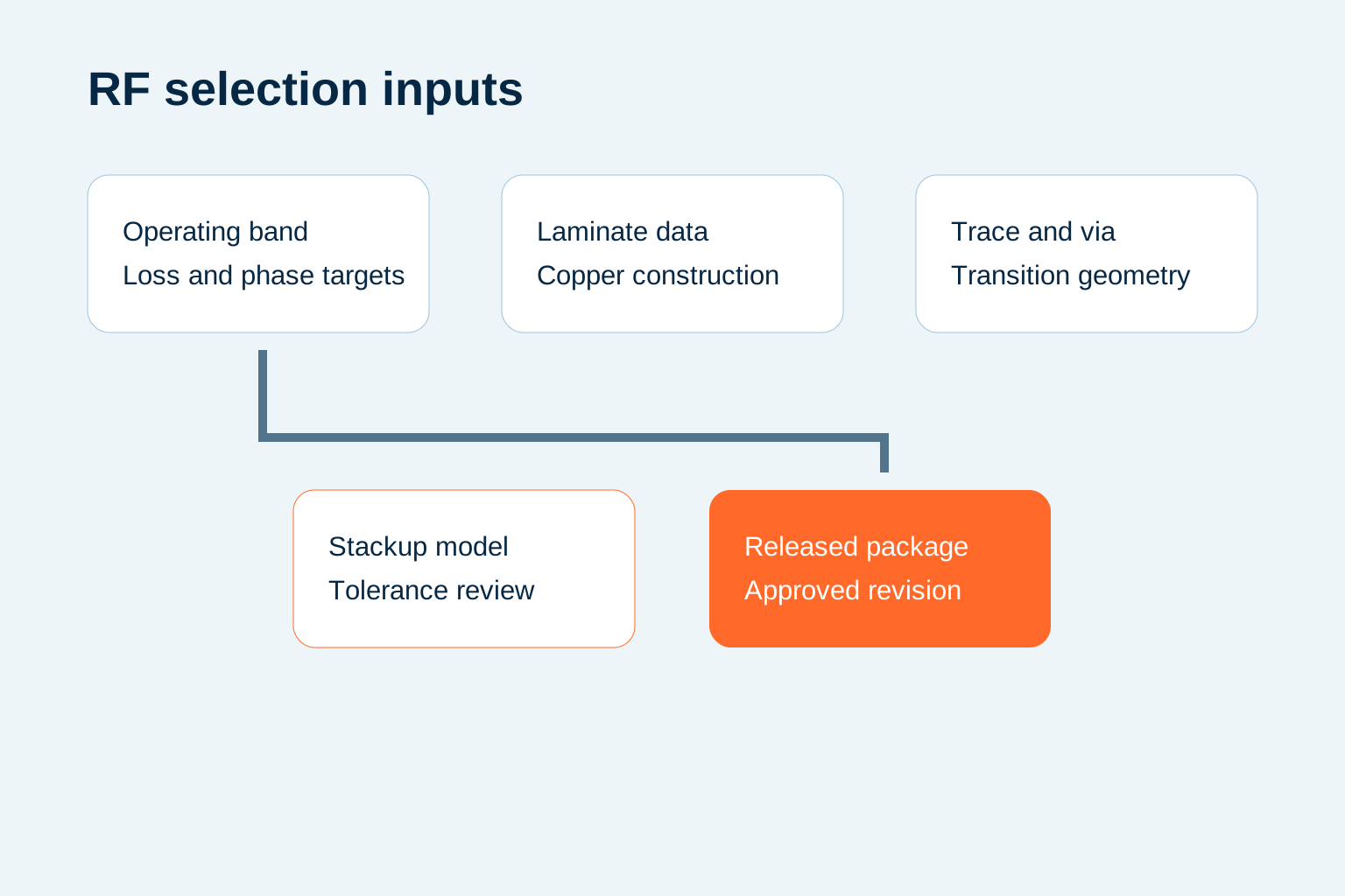
Record the operating band and the RF structures that cross the board: launches, filters, couplers, antennas, connectors, vias and transitions. Add the required characteristic impedance, permitted loss or phase variation, relevant interconnect lengths, power handling, temperature range and mechanical constraints. These inputs determine which material properties and process variations matter enough to control.
A low-loss label by itself does not establish suitability. A short interconnect at one band may tolerate a different construction from a long phase-sensitive path. Mixed RF and digital boards may also use a hybrid stackup, but laminate compatibility, copper balance, drilling, desmear, registration and lamination still need supplier review.
Keep three evidence sources separate
| Evidence source | What it contributes | What to record |
|---|---|---|
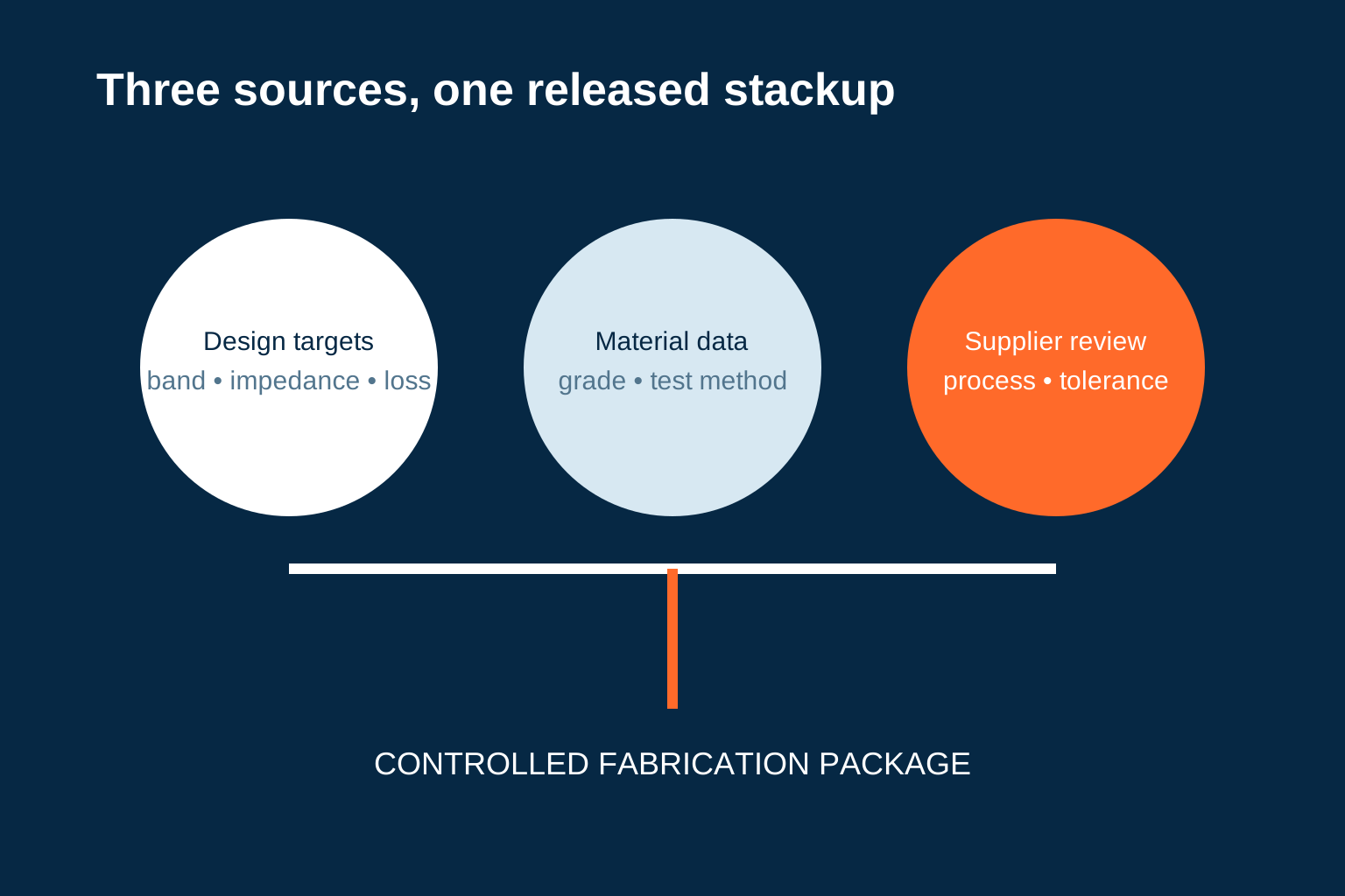
| Design model | Required electrical behavior for the actual geometry | Band, line type, impedance, loss/phase objective, ports and reference conditions |
| Material datasheet | Published dielectric, thermal and mechanical properties | Exact grade, thickness, copper option, test method, frequency and conditioning basis |
| Fabricator review | Buildable material set and process variation | Available construction, pressed thickness, copper treatment, tolerances, coupons and substitutions |
Compare laminate data on a common basis
Dielectric constant influences line geometry and propagation, while dissipation factor contributes to dielectric loss. Neither value should be copied without its test method and frequency context. Design values supplied for transmission-line modeling can differ from specification values used for material acceptance. Compare candidates only after aligning the data basis and the geometry in which it will be used.
Also review moisture behavior, glass transition or decomposition information where relevant, thermal expansion, copper adhesion, thickness availability and compatibility with the intended assembly environment. These properties do not all carry the same weight for every project; document which ones drive the shortlist.
Copper and finish are part of the RF structure
At higher frequencies, current concentrates closer to conductor surfaces, so copper profile can influence conductor loss. Rogers and Altium discussions both emphasize considering copper roughness together with dielectric and geometry. Specify a copper construction that can be sourced with the chosen laminate, and avoid translating a roughness label into a universal performance claim.
Finished copper, plating and surface finish can alter the modeled geometry or loss contribution. Identify whether the model uses base or finished copper and how plated features, connectors and launches are represented. The released drawing should make that basis explicit.
Compare stackup routes by their controlling trade-off
| Route | Why a team may evaluate it | Review before selection |
|---|---|---|
| Single laminate family | Simplifies the material system and modeling basis | Electrical fit, available thicknesses, copper pairing and total construction |
| Hybrid RF and conventional laminate | Places specialized material only where the RF channel needs it | Lamination compatibility, CTE relationship, symmetry, drilling and registration |
| Surface RF routing | Supports direct launches and accessible structures | Finish, copper profile, solder mask, reference continuity and environmental exposure |
| Internal RF routing | Can shield or integrate channels within a multilayer board | Pressed dielectric control, transitions, registration and test access |
Model traces, reference planes and transitions together
A stackup table is incomplete without the transmission-line geometry tied to it. State which layers carry each controlled structure, its reference plane, nominal trace dimensions and whether local copper, solder mask or cavities change the field. Via transitions need return-path continuity and a documented treatment of unused barrel, pads, antipads and any back-drill requirement.
Connector launches and component land patterns should be evaluated with the board transition rather than isolated from it. If electromagnetic simulation or test coupons are part of acceptance, define the model inputs, correlation method and owner before quotation.
RF stackup release flow
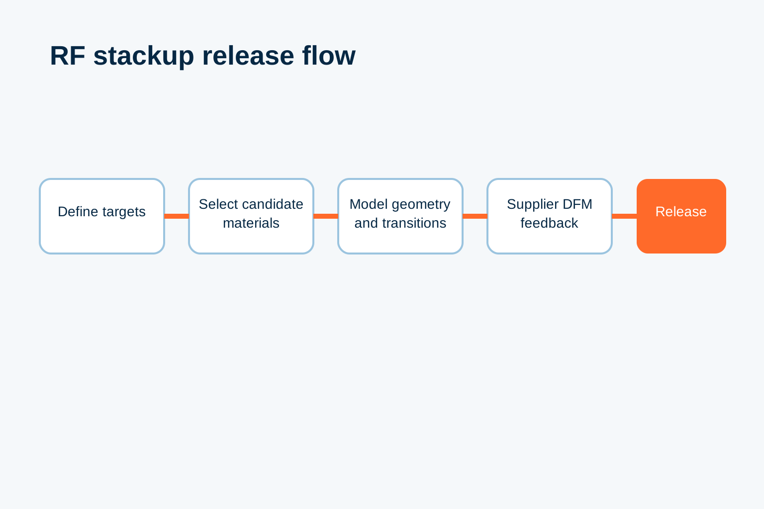
- Define bands, channels, line structures, impedance, loss/phase and environmental objectives.
- Shortlist exact laminate, dielectric-thickness and copper options on comparable data.
- Model traces, reference planes, launches and transitions in the candidate stackup.
- Send the proposal to the fabricator for material and process review.
- Resolve substitutions, pressed thickness, copper, tolerance and verification responsibilities.
- Release one controlled drawing, model basis and acceptance plan.
RF fabrication package checklist
- Exact material family or grade and permitted substitution process.
- Layer order, finished thickness, copper basis and dielectric construction.
- Controlled line type, target impedance and project-specific tolerance.
- Operating band and loss or phase requirement where these are acceptance inputs.
- Trace, launch, via, antipad, reference-plane and back-drill details.
- Copper foil/profile and surface-finish assumptions used in the model.
- Coupon, test method, reporting and acceptance responsibility.
- Revision history and approval owner for supplier-proposed changes.
Send the proposed stackup, material callout, Gerbers or ODB++, drill data, impedance table and any simulation or coupon requirement through Get a Quote. PCBArise can then review the package against the applicable PCB manufacturing route without turning a generic web value into a project promise.
Engineering review
Prepared and reviewed for project use
Engineering Director
Senior Quality Engineer
Review scope: technical accuracy, evidence wording, standards references, internal links and release readiness. Project requirements remain subject to the released files, applicable acceptance criteria and agreed test documentation.
FAQ
Questions engineers ask before release
What PCB material is best for RF circuits?+
There is no single best material for every RF circuit. Select from the operating band, channel length, impedance, loss and phase objectives, geometry, environment and available fabrication construction, using comparable supplier data.
Are low Dk and low Df always better?+
Not by themselves. Dk, Df, their test method and stability must be evaluated with the actual transmission-line geometry, copper and operating conditions. Mechanical, thermal and manufacturing requirements can change the appropriate choice.
Can RF laminate and FR-4 be combined in one PCB?+
A hybrid stackup can be evaluated when specialized material is needed only on selected RF layers. Lamination compatibility, expansion, symmetry, drilling, registration, pressed thickness and supplier process capability must be reviewed before release.
Why does copper roughness matter in an RF PCB?+
Copper surface profile can contribute to conductor loss as frequency increases. Its effect belongs in the same model as laminate properties, copper thickness, trace geometry and finish rather than being treated as a universal roughness limit.
What should an RF stackup drawing include?+
Include exact material and copper callouts, layer order, dielectric construction, finished thickness, controlled lines, target impedance and tolerance, transitions, finish, coupons or tests, substitution rules and revision ownership.
When should the PCB fabricator review an RF stackup?+
Involve the fabricator before release, after electrical targets and a candidate construction exist. The review should resolve material availability, buildable thicknesses, copper options, fabrication variation and verification responsibilities.
Reference points
Sources and verification starting points
External standards and industry references help frame the decision. Confirm current supplier evidence and project-specific requirements before release.
- Rogers Corporation — PCB fabrication and material considerations for 5G bands
- Rogers Corporation — selection of PCB materials for 5G
- Global Electronics Association — IPC-2221B public contents for generic printed-board design topics
- Altium — professional high-frequency material selection discussion
- Altium — professional copper-foil selection discussion
- Sierra Circuits — professional hybrid RF stackup workflow
- EMA Design Automation — professional RF PCB design overview