
Hydrocarbon ceramic
Low-loss rigid laminates suited to many RF, antenna and high-speed applications with familiar processing characteristics.
High frequency PCB manufacturing controls loss, impedance and phase behavior through RF laminate selection, copper profile, stackup and fabrication tolerances for RF and microwave PCB applications.
Frequency alone does not select an RF material. Insertion loss, Dk stability, dissipation factor, copper roughness, thermal exposure and fabrication compatibility all matter.
Low-loss rigid laminates suited to many RF, antenna and high-speed applications with familiar processing characteristics.
A material family for demanding microwave and millimeter-wave circuits that requires dedicated fabrication controls.
Place low-loss material only on the signal layers that need it while using FR-4 elsewhere in the stack.
Connector transitions, ground-via pitch and reference continuity are treated as part of the transmission structure.
The material datasheet, modeled stackup and launch geometry should agree before tooling. Substituting an “equivalent” laminate without electrical review can change the circuit.
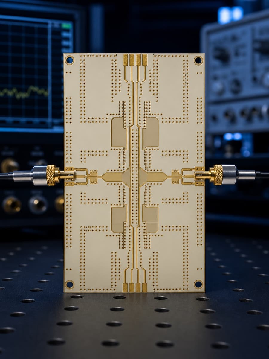
RF and microwave construction reference
| Material systems | Rogers, Taconic, PTFE and ceramic-filled hydrocarbon laminates |
|---|---|
| Construction | All-RF or hybrid RF / FR-4 stackups |
| Minimum trace / spacing | 2.5 / 2.5 mil standard; advanced geometry by review |
| Controlled impedance | ±10% standard; ±5% for tighter requirements |
| Copper profile | Standard, low-profile or rolled copper as material and loss model require |
| Via structures | Through, blind, buried, back-drilled and via-fence structures |
| Surface finish | ENIG, ENEPIG or application-specific RF finish |
| Material control | Manufacturer, grade, thickness, Dk and Df locked by drawing |
| Verification | Electrical test and impedance coupon when specified |
Capability values are design-dependent. Material, copper weight, layer count, via structure, finished thickness and surface finish can change the achievable combination.
The modeled geometry must use the selected laminate’s design Dk, dielectric thickness and copper profile. Return-path discontinuities can undo a correct trace calculation.
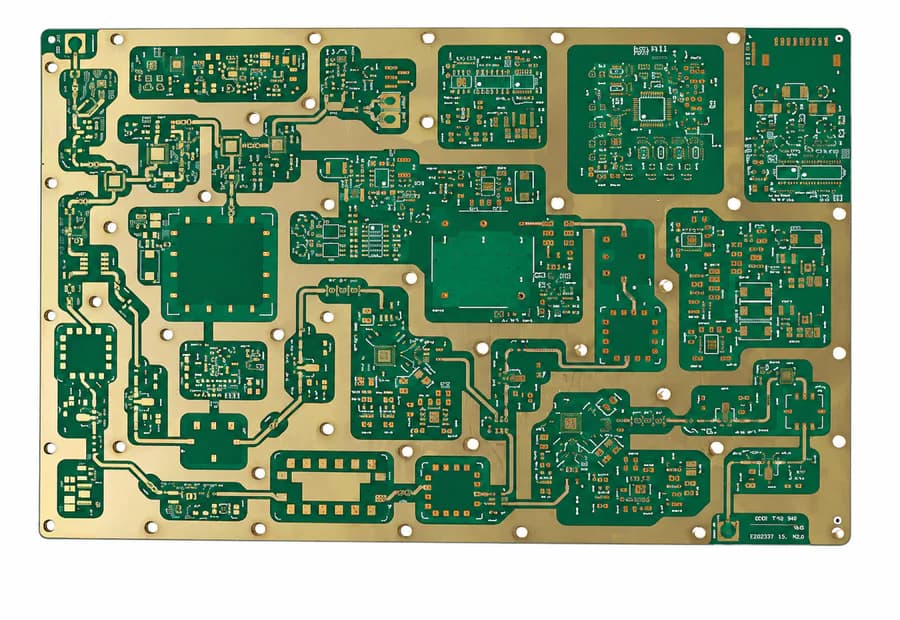
Align laminate Dk and Df, copper profile, dielectric thickness, launch geometry, via fences and impedance verification.
Use these examples as a starting point. The board construction still follows the product’s electrical, mechanical and qualification requirements.
RF front ends, filters, amplifiers and antenna distribution networks.
Millimeter-wave radar antennas and signal paths requiring stable low-loss material behavior.
Patch arrays, feed networks and phased-array structures with phase-sensitive geometry.
Microwave links and compact RF assemblies where loss and mass are constrained.
Calibration, instrumentation and high-frequency interconnect boards.
Low-loss channels and mixed RF-digital stackups with controlled return paths.
Quality documents
The published ISO records name Zhongshan Wenquan Electronic Manufacturing Co., Ltd. and its Zhongshan PCBA facility. They do not certify every PCBArise facility, service or product.
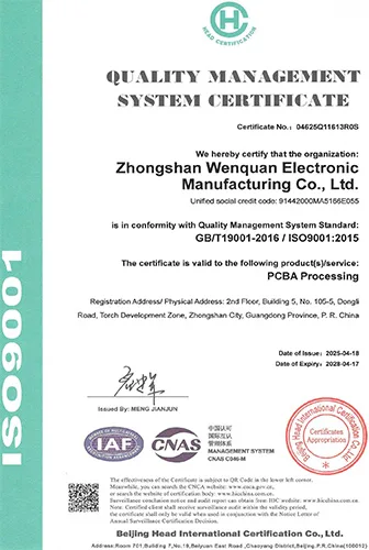
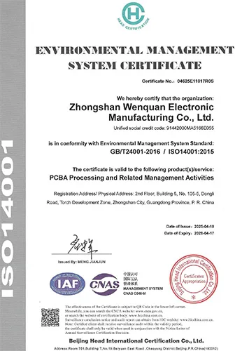
These are management-system certificates, not product or batch COAs. No batch inspection reports or COAs are currently published here.
These answers cover RF laminate selection, hybrid stackups, impedance control and fabrication review.
A high-frequency PCB uses a material and stackup selected for controlled dielectric behavior and signal loss. RF and microwave applications require the laminate, copper profile, impedance geometry, via transitions, connector launches and surface finish to support the same electrical objective.
Yes. Rogers materials are supported together with Taconic, PTFE and other controlled-Dk laminate systems. The exact grade and thickness should be fixed in the fabrication drawing.
Yes. A hybrid stackup can reserve low-loss material for RF layers and use FR-4 elsewhere. Lamination compatibility, thickness, symmetry and registration still require engineering review.
Available controlled-impedance tolerance is confirmed from the exact material, stackup, copper geometry, coupon plan and project acceptance requirement. Include the target and tolerance in the fabrication package for engineering review.
Continue to multilayer, HDI, capability limits or DFM review according to the RF construction.
Share the available Gerber, ODB++, drawing, stackup or project requirements with the PCBArise team.