
In short
For fine-pitch PCB assembly, do not apply one blanket solder-mask expansion everywhere. Start with the component maker’s land pattern, calculate the opening and remaining mask web using the fabricator’s registration allowance, and decide whether an NSMD or mask-defined pad is appropriate for that package. Preserve a stable dam where the design permits it; where it does not, make the controlled exception explicit rather than leaving the fabricator to guess.
- Solder-mask opening, pad size and the remaining mask web must be checked together; optimizing only one produces a fragile footprint.
- Use the package land-pattern source first, then apply a fabrication registration allowance that the chosen process can support.
- For very dense BGAs and fine-pitch parts, a mask-defined strategy can be more robust than forcing an unsupported narrow mask sliver.
- Send separate solder-mask data and clear exceptions for vias, exposed copper and special pads; do not hide them in a generic note.
Fine-pitch solder-mask design is a three-way trade: expose enough pad to solder, allow for mask registration movement, and leave a mask dam that will survive fabrication and assembly. The right drawing does not start with a universal expansion number. It starts with the component land pattern, pad-to-pad spacing and the fabricator’s published solder-mask capability. If those values leave no stable web, change the footprint strategy or make the exception explicit before the Gerber files leave design.
What should solder mask do around fine-pitch pads?
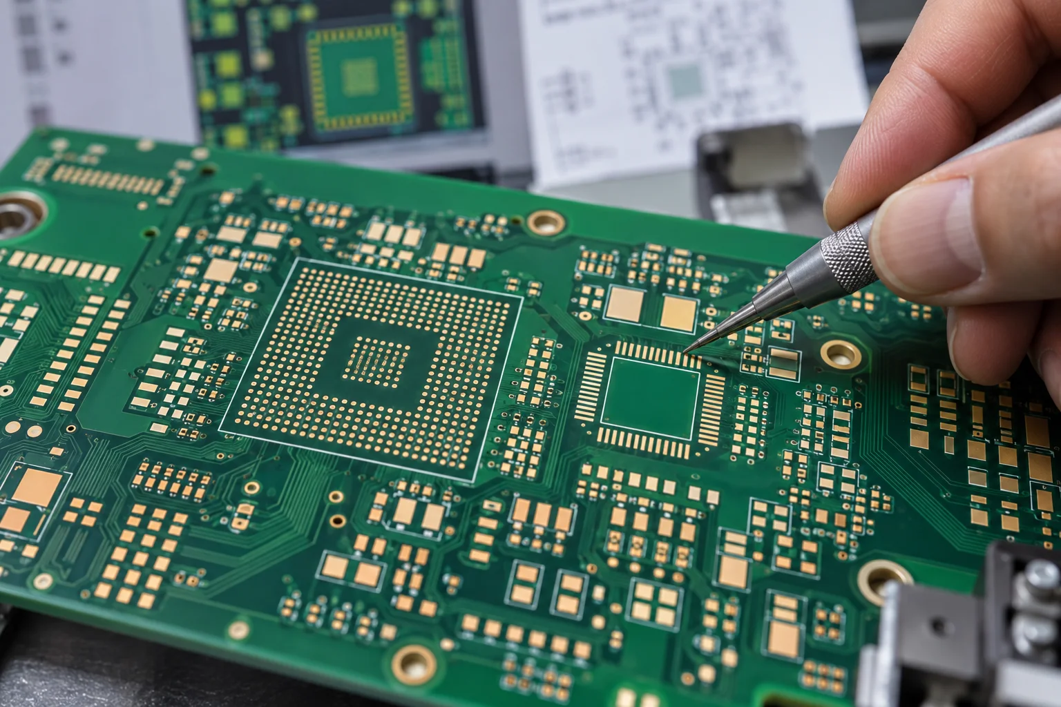
Keep solder on its intended land while keeping adjacent copper protected. On a normal non-solder-mask-defined (NSMD) land, the mask opening is larger than the copper pad so the solder joint can wrap the copper edge. On a solder-mask-defined land, the mask overlaps the copper edge and defines the exposed pad. Neither is universally better: NSMD is common where spacing supports a robust opening and dam; mask-defined lands can help preserve separation when a dense package leaves too little room for a free-standing sliver of mask.
IPC’s QFN guidance illustrates the arithmetic. It describes common mask opening clearance in the 60–75 µm range to accommodate registration, while noting that a 0.4 mm-pitch package with 250 µm lands may not leave a practical mask web between lands. Those are illustrative design constraints, not a claim that every PCBArise build uses those numbers. The actual allowable opening and web must come from the selected fabrication process and package documentation.
| Decision | What to check on the footprint | What can go wrong if it is ignored |
|---|---|---|
| Mask opening | Pad size plus the registration allowance on every side; check against nearby copper, not only the pad. | Too small can clip the solderable land; too large can erase the intended dam or expose neighbouring features. |
| Mask dam / web | Remaining mask between adjacent openings after expansion, compared with the fabricator’s stable minimum. | A narrow sliver can detach or disappear, letting solder bridge between fine-pitch leads. |
| Pad definition | Whether the component’s land-pattern recommendation calls for NSMD or mask-defined pads at this pitch. | Changing pad definition casually changes the exposed copper geometry and solder-joint behaviour. |
| Vias and copper nearby | Tenting, plugging or keep-out treatment for vias and traces near the package. | Unexpected exposed copper or an open via can attract solder or reduce isolation. |
How do you calculate whether a mask dam remains?
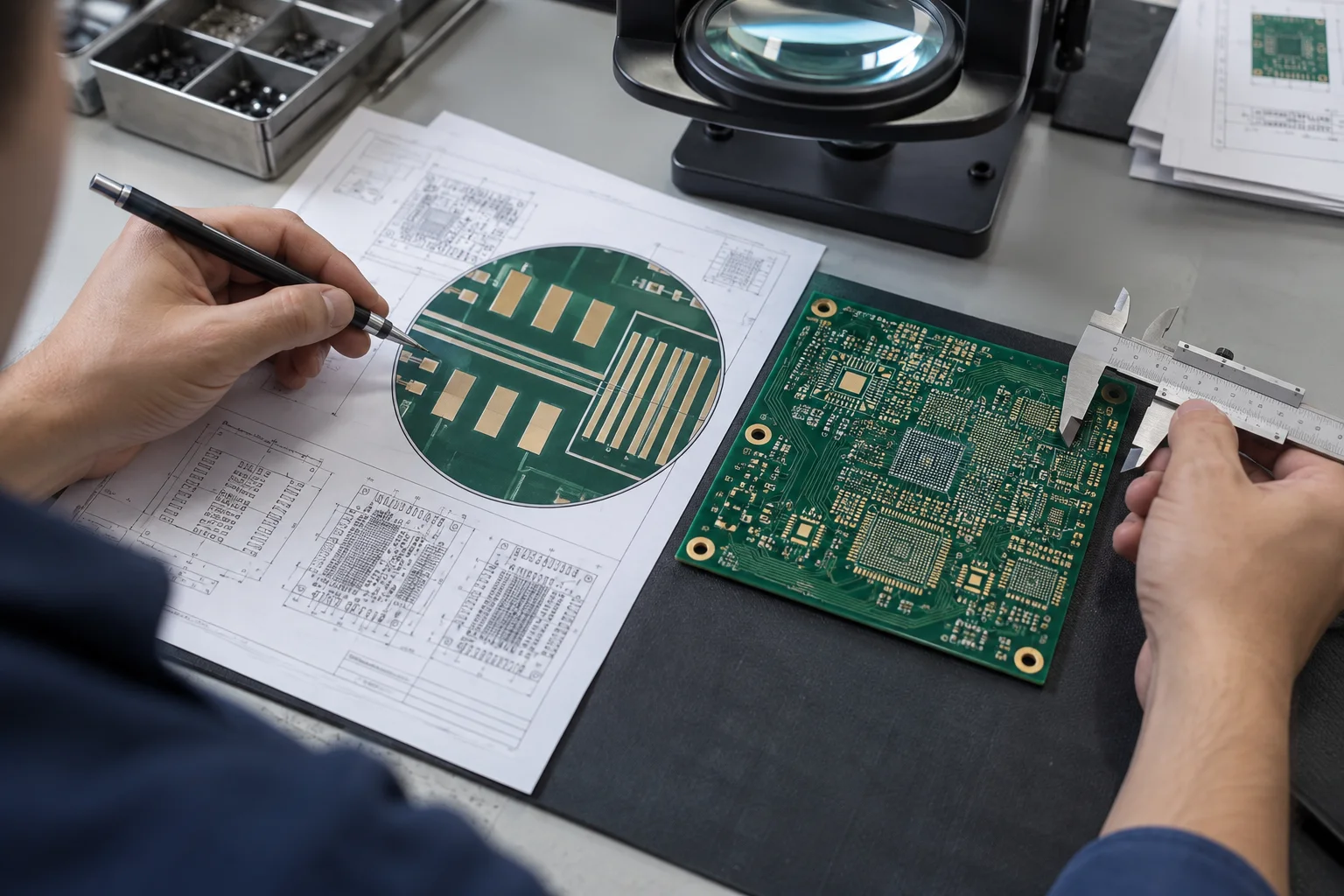
Use the pad-to-pad copper gap and subtract the opening expansion from both neighbouring pads. In simplified form: remaining mask web = copper gap − expansion on pad A − expansion on pad B. For equal pads using the same expansion, that becomes copper gap minus twice the expansion. Then compare the remaining web with the fabricator’s process minimum, not with a value copied from an unrelated board.
That calculation is only a first filter. It must be repeated at corners, around vias, and where a local rule changes a pad opening. It also assumes the copper land pattern is valid for the component. The component manufacturer’s recommended footprint and an applicable land-pattern standard are the starting point; a DFM rule should catch contradictions before fabrication, not redesign a package interface after release.
For example, if a footprint can retain a stable web with its required registration allowance, keep an NSMD strategy where the land pattern calls for it. If the calculation leaves a sliver below the process limit, do not simply reduce the allowance to make the DRC quiet. Evaluate a mask-defined pad, a package-specific zero or reduced expansion rule, a layout change, or a fabrication process whose stated registration can support the required geometry. The Altium ultra-HDI discussion makes the same distinction: tight geometry turns solder mask into a first-order design constraint.

When should a pad be mask-defined instead of NSMD?
Use the package and spacing constraint to decide, not a site-wide default. NSMD pads are widely used because the solder joint can wrap the pad edge, but the opening needs enough registration allowance and a durable dam. At very fine BGA or QFN geometry, a mask-defined opening can hold the exposed copper inside a controlled aperture and preserve separation. This is a package-specific choice: changing it alters the final solderable pad size, so it must agree with the component supplier’s guidance and the assembly process.
Do not confuse mask-defined pads with “mask over every via.” Vias near a fine-pitch land need their own instruction—tented, filled and capped, plugged, or left open—based on whether they can wick solder, create a paste-printing issue or serve an electrical function. For solderable via-in-pad, the related via-in-pad guide explains why an open hole is not a safe default.
What data should go into the fabrication package?
Send solder-mask layers in the manufacturing outputs and add a drawing note that tells the fabricator where the ordinary rule stops. The note should name the normal expansion basis, the minimum acceptable dam or process reference, any package-specific override, the handling of vias near fine-pitch pads, and which component footprints are locked to the supplier drawing.
Solder mask: use the released mask layers as the governing geometry. Apply [normal rule/process reference] except at [package references], where the released local opening and pad-definition strategy are required. Do not merge adjacent openings or remove a mask dam without reporting the affected designators. Treat vias in [named areas] as [tented / filled and capped / other released instruction].
This gives a P1 design or NPI engineer an answer to the real handoff question: what must be preserved, and what fabrication adjustment is acceptable? It is more useful than a vague “fine-pitch solder mask required” note, which says nothing about opening geometry or ownership.
How do mask, paste and assembly work together?
Solder mask defines where copper remains covered; a stencil defines where paste is deposited. A correct mask opening does not set paste volume, and a smaller mask opening should not be compensated by blindly enlarging a stencil aperture. Review paste apertures for the package, thermal pad and component-body constraints separately, then check the whole set in the assembly DFM review.
Fine-pitch failures usually appear at the interfaces: a lost mask dam can give solder a path to bridge; a clipped opening can reduce solderable area; an exposed trace near a pad can collect paste; an open via can drain solder. The recent UHDI Consortium announcement records why increasingly dense geometries are driving fresh work on aperture, paste and inspection data. That news is background, not a specification for this board: your released footprint and the selected process remain the design authority.

Four mistakes that create avoidable fine-pitch risk
- One expansion rule for every pad: a connector, BGA, QFN and test pad can require different mask treatment. Use targeted rules with a documented reason.
- Keeping a cosmetic mask sliver: a line that looks present in CAD may be below the fabrication process’s stable minimum. Check the manufactured web.
- Using a generic “fine-pitch” note: it does not state opening, pad definition, via treatment or who can change them.
- Mixing up solder mask and paste mask: each controls a different physical feature and must be reviewed independently.
Before releasing a dense board, send the Gerber or ODB++ data, fabrication drawing, component land-pattern references, BOM, placement data and any intended stencil or inspection requirements. The SMT assembly page provides the service context; the geometry in the released design package determines what can be manufactured and assembled.
About the author
PCBArise Electronics
PCBArise Electronics publishes this guide to help design and NPI teams prepare clearer manufacturing files. The requirements for any actual build are confirmed from its current design package.
FAQ
Common questions
What solder mask expansion should I use for a fine-pitch PCB?+
Use the component land pattern plus the selected fabricator’s registration allowance, then verify the remaining mask dam everywhere it matters. There is no safe universal number: a value that works on a coarse connector can remove the dam between dense BGA or QFN pads.
What is a solder mask dam?+
A solder mask dam, or web, is the strip of solder mask left between adjacent mask openings. It helps keep copper protected and solder separated. For fine pitch, calculate the manufactured web after both adjacent openings expand and compare it with the fabrication process limit.
Should fine-pitch pads be NSMD or solder-mask-defined?+
Follow the component’s land-pattern recommendation first. NSMD pads are common when spacing supports a robust opening and dam; mask-defined pads can be appropriate when dense geometry needs the mask to define the exposed pad. Treat the choice as a package-specific footprint decision, not a global preference.
Can I use zero solder mask expansion to save a mask dam?+
Only when the footprint, registration capability and process plan support it. Zero expansion may preserve separation, but it reduces tolerance for mask-to-copper misregistration. Apply it as a documented local rule after checking the package and fabrication process, not as an automatic fix for every DRC violation.
Does solder mask prevent all fine-pitch solder bridges?+
No. A good mask dam helps isolate adjacent lands, but bridges also depend on pad geometry, paste volume, stencil aperture, component placement and reflow. Review those inputs together; a mask rule cannot compensate for an unsuitable footprint or excessive paste deposit.
Technical references
Sources used for this guide
These sources explain the standards, materials or process details discussed above. Check the current revision when applying them to a new design.