
In short
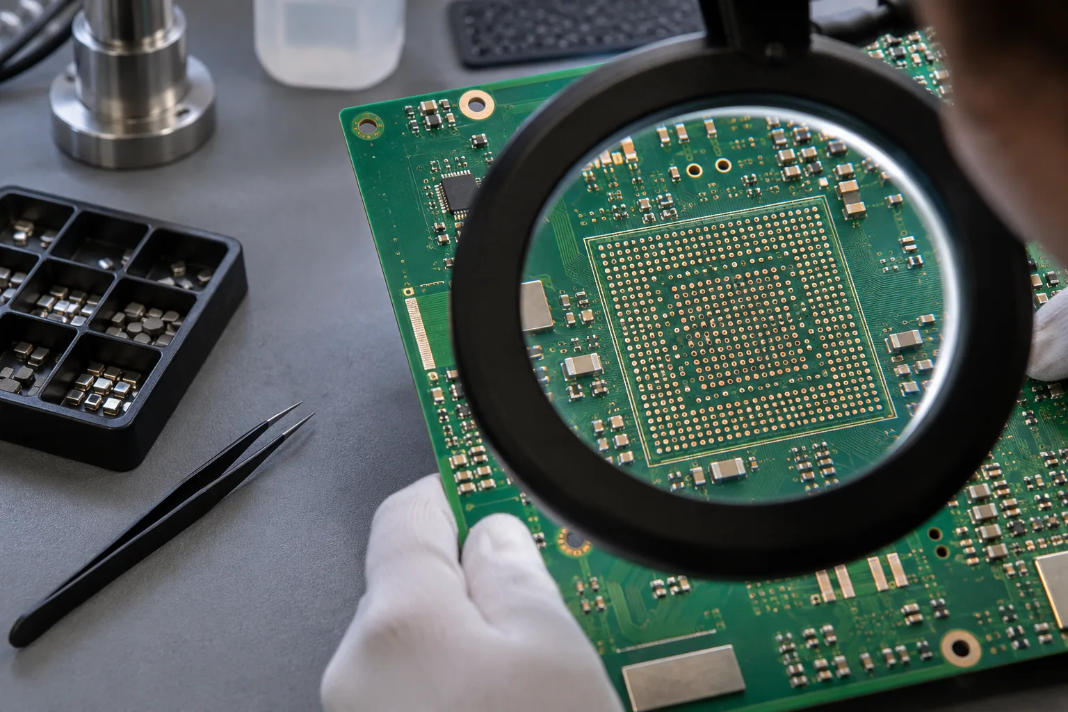
Via-in-pad and microvia are not competing via types. Via-in-pad means the hole opens inside a component pad; a microvia is a small blind HDI interconnect, usually laser formed. A microvia can sit in a pad, and a mechanically drilled via can too. Start with the BGA escape geometry and layer transition; use an off-pad dogbone when it fits, and specify filled, planarized, capped pads where solderable via-in-pad is needed.
- Decide pad location and via structure separately; “microvia” does not automatically mean “in-pad.”
- Use an off-pad dogbone when pitch and routing space allow it; move into the pad only when escape geometry requires it.
- For solderable via-in-pad, define the fill, planarization and cap construction so solder does not wick into an open hole.
- Show start/end layers and stacked or staggered relationships for each microvia path.
First separate two questions: is the via opening inside a solderable pad, and what kind of interconnect connects the layers? “Via-in-pad” answers the first; “microvia” answers the second. A laser-drilled microvia may be in a BGA pad or outside it. A conventional drilled via may also be in a pad, although its larger hole and fill/cap construction can make it costly. Treating the terms as a simple either/or hides the actual escape-routing choice.
How do via-in-pad and microvia overlap?
A via-in-pad places a plated via opening within a surface-mount land. A microvia is a short, small HDI via used to connect adjacent or nearby layers, commonly produced by laser drilling in a sequential-lamination build. One describes location; the other describes structure. Sierra Circuits’ via-in-pad guide discusses the pad location and solder-wicking concern, while Altium’s microvia guide covers the HDI layer connection.
| Layout choice | Pad location | Via structure | Useful when | Main manufacturing consequence |
|---|---|---|---|---|
| Dogbone escape | Via outside pad | Often mechanical through via | Pitch leaves room for short trace and annular ring | Usually avoids filled/capped solderable pad, but consumes escape space. |
| Mechanical via-in-pad | Via inside pad | Drilled plated via, possibly through board | Pad escape needed and larger hole/stackup is workable | Solderable pad needs an agreed fill, planarization and cap approach. |
| Off-pad microvia | Via outside pad | Blind HDI microvia | Fine escape or shallow layer transition without using the land | Adds HDI build steps but may leave the pad uninterrupted. |
| Microvia-in-pad | Via inside pad | Blind HDI microvia | Fine-pitch BGA has too little room for an off-pad escape | Combines HDI build steps with a solderable pad that needs a specified surface finish and via treatment. |
These are layout patterns, not universal process quotes. The board thickness, BGA pitch, pad diameter, layer count and available route channels determine whether a chosen pattern fits.
Which escape should you draw for a fine-pitch BGA?
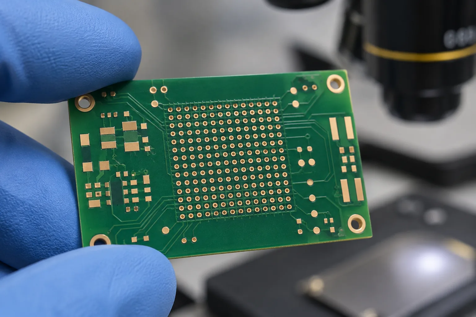
Use a dogbone to an off-pad via if the pad pitch leaves enough copper clearance and trace width. It keeps an open hole away from the solder land and typically avoids a filled/capped pad. If a dogbone violates spacing or blocks inner rows, move the transition into the pad and define its construction. If the signal needs only a short blind transition, a microvia-in-pad can free more routing channels than a through via. Do not choose microvia solely because it sounds smaller; a conventional via outside the pad may already solve the escape.
For example, on a dense BGA, outer rows may escape with short dogbones while inner rows need a L1–L2 microvia in the pad. That hybrid is often more economical than converting every pad to HDI via-in-pad. It is an illustrative routing example, not a PCBArise process capability statement.
What must a solderable via-in-pad note say?
Do not leave the opening unaddressed in a solder land. An open via can draw solder away from the joint and create an uneven pad. Specify the via location and finished pad requirement, the intended fill, planarization and cap construction, and the acceptance basis. IPC-4761’s via-protection taxonomy provides covering and filled/capped terminology; the actual drawing should state the selected treatment instead of merely writing “via-in-pad.”
Example fabrication note (illustrative): “U1 BGA pads marked VIP require filled, planarized and copper-capped vias before surface finish. Preserve a solderable, level land. Show via start/end layers on the drill map and identify these pads separately from ordinary tented vias.”
Replace “U1” and the required construction with your real design. A thermal via in a large exposed pad, a fine-pitch BGA pad and a test pad can need different solder-mask and fill strategies; never apply one blanket via note to every hole.
When do stacked microvias change the decision?
A single L1–L2 microvia is not the same build as multiple microvias stacked vertically through sequential layers. Stacking can compress the escape footprint, but increases process and reliability demands at the interfaces. Staggering the next microvia shifts the joint laterally and may need more routing area. IPC’s microvia reliability warning focuses on latent failures at stacked interfaces in high-performance products. Show each via’s start and end layer and whether the transitions are stacked or staggered so the fabrication route is not inferred from a 2D pad view.

A compact drawing and file handoff
- Mark BGA pitch, pad diameter, solder-mask opening and which positions contain in-pad vias.
- Provide a layer-by-layer drill map: mechanical/laser method, via start and end layers, and stacked or staggered relationships.
- Call out fill, planarization, copper cap and finished solderable pad requirements for relevant in-pad vias.
- Keep ordinary tented vias, thermal vias and solderable via-in-pad structures in distinct notes.
- Check the routing and stackup together; an HDI layer transition changes both fabrication sequence and available signal layers.
The HDI PCB page provides service context and the BGA assembly page covers the assembly side. This guide's decision is earlier: choose where the via sits and how it connects layers, then make that combination explicit in the fabrication files.
About the author
PCBArise Electronics
PCBArise Electronics publishes this guide to help design and NPI teams prepare clearer manufacturing files. The requirements for any actual build are confirmed from its current design package.
FAQ
Common questions
Is via-in-pad the same thing as a microvia?+
No. Via-in-pad names the via’s location inside a component land; microvia names a small HDI layer connection. A microvia can be in-pad or off-pad, and a mechanically drilled via can also be placed in-pad.
When should I use dogbone routing instead of via-in-pad?+
Use a short dogbone to an off-pad via when BGA pitch and clearances allow it. It leaves the solderable pad uninterrupted. Move into the pad when the dogbone cannot meet routing geometry or blocks access to inner rows.
Does every via-in-pad need filling and copper capping?+
No. For a solderable fine-pitch land, specify a filled, planarized and capped construction so the pad stays level and solder cannot wick into an open hole. Other pad functions may use different covering; identify them separately on the drawing.
Can a microvia be outside the component pad?+
Yes. An off-pad blind microvia provides a shallow HDI transition while leaving the component land clear. Check the available annular ring, trace escape and layer transition before deciding its position.
Are stacked and staggered microvias equivalent?+
No. Stacked microvias align vertically and compress routing space but add interface-reliability concerns; staggered microvias shift laterally and use more area. Show the start/end layer and arrangement for each transition in the drill map.
Technical references
Sources used for this guide
These sources explain the standards, materials or process details discussed above. Check the current revision when applying them to a new design.