

In short
Give every release-critical net a named, reachable target before layout is frozen. ICT favors repeatable fixture-side access on a consistent grid; flying probe accepts more varied target locations but still needs clear approach paths, stable board support and an executable netlist. Define target geometry with the chosen test process, then publish a test-point schedule instead of relying on unlabeled copper.
- Prioritize power, ground, programming, reset, clocks, communication and safety-monitoring nets before convenience signals.
- A valid target needs conductive area, probe approach, component clearance and board support—not only a test-point symbol.
- Keep the schematic test-point ID, net name, PCB pad and test documentation synchronized.
- Use a test-point schedule to state side, target type, access limits and intended method without inventing universal dimensions.
Place test points where a real probe can approach, land and remain stable—not wherever a test-point symbol fits. Start with the nets that decide safe power-up, programming and failure diagnosis. Give each target a schematic ID, net name, PCB location, access side and intended test method. ICT usually benefits from consistent fixture-side targets; flying probe can reach a more varied pattern, but component height, probe angle, board edge and support still limit access.
What makes one test point usable for both ICT and flying probe?
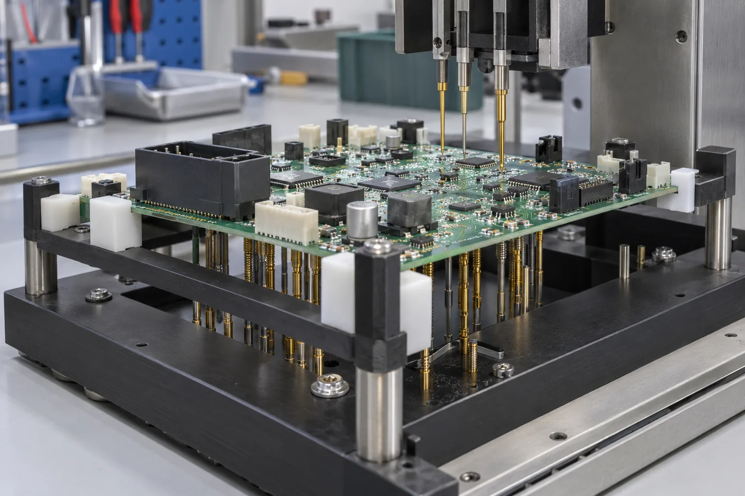
A shared target needs exposed conductive area, a clear probe path, enough local spacing to prevent accidental contact, and mechanical support beneath the probe load. ICT approaches through a fixed bed of probes, so target position must agree with the fixture plate and board locators. A flying probe moves between targets, which reduces dedicated fixture hardware but does not remove collision, shadowing or stability limits.
| Design question | ICT fixture | Flying probe | Shared layout action |
|---|---|---|---|
| Target pattern | Benefits from a regular fixture-side pattern and repeatable datum. | Can use varied coordinates within machine travel and approach limits. | Export exact X/Y, side, net and target type. |
| Probe path | Fixed probe body and fixture plate need clearance. | Moving head needs a collision-free approach around tall parts. | Keep component bodies, solder and hardware out of the access envelope. |
| Board support | Support prevents bowing under many simultaneous probes. | Support stabilizes the board as individual probes land. | Identify safe support zones and underside conflicts. |
| Revision change | May require fixture and program updates. | Usually requires coordinate/program regeneration. | Tie every access file to the same board revision. |
How should size, spacing, grid and board-edge position be specified?
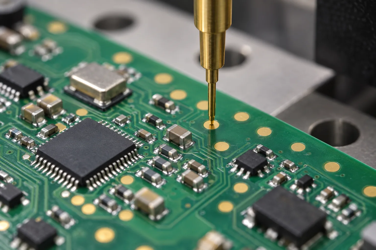
Specify the target from the selected probe, fixture construction, board tolerance, surface finish and access side; do not copy one universal pad diameter or pitch. A target that looks large in CAD can lose usable landing area after mask registration, nearby solder, via geometry or positional tolerance is considered. A dense grid can also leave too little room for probe barrels, wiring or support pins even when the copper pads themselves do not overlap.
Record the finished exposed target, not only the nominal copper. For each target family, state pad shape, mask opening, permitted via use, side, minimum clear approach envelope and any no-probe edge region. The fixture designer can then select a compatible probe and locator scheme from actual geometry. If the target is near a routed edge, connector, clamp, tooling hole or breakaway tab, show that feature in the same mechanical view.
Which dimensions belong in the handoff?
Put exact target geometry in the PCB data and put access assumptions in the test-point schedule. The schedule should identify whether the point is a dedicated pad, accessible via, connector pin or component lead; whether it is top, bottom or either-side access; and which physical feature can obstruct the probe. This makes a missing dimension visible without pretending that one house rule fits every tester.
Which nets should receive test points first?
Protect nets that control safe startup, programming and diagnosis before adding general signal coverage. Begin with ground references and every independent supply rail, including enable and power-good signals. Then add reset, boot-mode, programming/debug, clocks, buses and communication interfaces. Include safety-monitoring or interlock nets that can prevent power-up. Use remaining access for diagnostic nodes whose absence would make likely faults expensive to isolate.
| Priority | Net group | Why access matters | Useful handoff detail |
|---|---|---|---|
| 1 | Ground and supply rails | Establish references and detect shorts before powered testing. | Rail name, expected relationship and current-limited power sequence. |
| 2 | Reset, boot, enable, programming and debug | Recover or configure a board that cannot start normally. | Required state, connector alternative and firmware dependency. |
| 3 | Clocks, buses and external interfaces | Separate assembly faults from configuration or communication faults. | Relevant endpoint, access method and inactive-state caution. |
| 4 | Diagnostic analog and control nodes | Localize failures that end-point functional test cannot isolate. | Expected static range or comparison condition when known. |
When do double-sided access, probe shadow and component height block testing?
They block testing when the probe body or fixture structure cannot reach a target without colliding, bending the board or touching an adjacent conductor. A bottom target beneath a tall top-side connector can conflict with a support post or clamping plate. A top-side target beside a shield, heat sink or large electrolytic can be visible in CAD yet inaccessible to an angled moving probe. Test both sides as mechanical assemblies, not as isolated copper layers.
Double-sided fixtures can increase access, but they add alignment, support, wiring and maintenance work. Use them only when the inaccessible nets justify that complexity. Before freezing the layout, overlay keepouts for probe bodies, support pins, locators, clamps and moving-head clearance. Reserve datum and board-edge features that let every unit seat the same way.
What should be written in the schematic, netlist, PCB and test documents?
Use one test-point identity across every file and add the physical and electrical attributes each downstream step needs. The schematic carries the TP designator, net name and intended diagnostic function. The PCB carries the pad, side, mask opening and mechanical clearance. The IPC-356/netlist or equivalent electrical data establishes connectivity. The test-point schedule connects that electrical identity to coordinates, target type, priority, intended method and any safe-state note.
Example drawing note: “Test access is defined by schedule [file/revision]. Each listed target shall retain its TP designator, net name, access side and exposed landing feature in the released PCB data. Keep the stated probe-access envelope free of component bodies, hardware and panel features. Regenerate fixture and flying-probe coordinates after any layout revision that moves a listed target.”

What should a test-point schedule contain?
Give the test engineer a row that can be mapped without interpretation. Recommended columns are TP ID, net name, X, Y, side, target type, exposed dimensions, priority, intended method, expected unpowered condition, access note and source PCB revision. Add connector alternatives when a net should be reached through a product interface rather than a dedicated pad.
Copyable row: “TP_[ID] | [NET] | X=[coordinate] | Y=[coordinate] | [top/bottom] | [pad/via/connector] | exposed target=[dimensions] | priority=[1–4] | method=[ICT/flying probe/both] | condition=[unpowered check] | access note=[keepout/support] | PCB rev=[rev].”
Five layout mistakes that turn access into a test failure
- Counting a via as accessible without checking finish and mask: its usable landing surface may be smaller or covered.
- Placing targets under tall or overhanging parts: a moving probe or fixture barrel can be shadowed even when the pad is visible from above.
- Ignoring board support: probe force can deflect a thin or cut-out area and create intermittent contact.
- Renaming nets between schematic and test files: coordinate data becomes difficult to map and diagnose.
- Changing target coordinates without a revision trigger: the old fixture or program can contact the wrong feature.
Use the test-method comparison to choose the evidence you need, then carry the selected access into the PCB design and assembly testing handoff. The next useful artifact is the completed test-point schedule, not a generic coverage claim.
About the author
PCBArise Electronics
PCBArise Electronics publishes this guide to help design and NPI teams prepare clearer manufacturing files. The requirements for any actual build are confirmed from its current design package.
FAQ
Common questions
Can the same PCB test point serve ICT and flying probe?+
Yes, when both systems can reach the exposed conductive target without collision or unstable board deflection. Record its coordinate, side, target type and access envelope; the same copper feature is not automatically usable by both probe geometries.
What size should an ICT test point be?+
Set the exposed target from probe-tip geometry, fixture and PCB positional tolerances, surface finish, mask registration and adjacent-feature clearance. Publish the actual pad and mask opening in the PCB data instead of applying one universal diameter to every board.
Which nets need PCB test points first?+
Prioritize ground, each power rail, enable and power-good, reset, boot, programming/debug, clocks, communication interfaces and safety-monitoring nets. Add diagnostic nodes where end-point tests would otherwise make likely faults difficult to isolate.
Do flying probes eliminate test-point rules?+
No. They reduce dedicated bed-of-nails hardware, but still require reachable conductive targets, collision-free approach paths, board support, accurate coordinates and a program tied to the correct netlist and board revision.
What files should accompany a PCB test-point design?+
Provide the schematic with TP IDs and net names, PCB fabrication and assembly data, connectivity/netlist data, X/Y coordinates with access side, a test-point schedule, mechanical keepouts and the test requirement or program input tied to the same revision.
Technical references
Sources used for this guide
These sources explain the standards, materials or process details discussed above. Check the current revision when applying them to a new design.
- Keysight — ICT access, fixture and coverage factors
- Keysight — ICT fixture and probe integrity
- IPC technical paper — test targets, probe selection and fixture maintenance
- IPC technical paper — test-probe assignment and flying-probe optimization
- SPEA — electronic-board test method context
- Seica — flying-probe access and CAD-driven test context