
Requirements and interface review before schematic or layout work is assigned
PCB Manufacturing / engineering service
PCB Design Services
PCB design services connect product requirements to a manufacturable board package. The engineering review can cover design inputs, stackup and material planning, component decisions, design for manufacturing (DFM), design for assembly (DFA) and the file set needed to move the released design into PCB fabrication and assembly.
ScopeRequirements to release
StackupLayer and material plan
DFM / DFAFabrication and assembly fit
HandoffReleased production files
For stackup, layout checks and release files, use the PCB design guide.
Service scope
PCB Design Service Scope
A useful PCB design service starts by defining what is already available and what engineering work is required. The scope can be reviewed around the design phase, board technology, product constraints and the files expected at handoff.
Component, package, availability and lifecycle considerations connected to the intended build
Layer count, stackup, material and copper planning for the electrical and mechanical requirements
DFM and DFA review before the design is released for fabrication or assembly
Design revision, approval and change notes kept with the manufacturing handoff
A defined boundary between PCB design support, customer-owned IP and production engineering
Technical reference
PCB Design Inputs and Deliverables
The exact package depends on whether the starting point is a product requirement, schematic, reference design or an existing board revision. The table makes missing inputs visible before the schedule is committed.
PCB Design Service Inputs and Deliverables
Define the design boundary before engineering work begins
| Design inputs | Requirements, interface list, enclosure constraints, power targets and applicable product conditions |
|---|---|
| Source data | Schematic, reference design, component list, mechanical files and customer design rules as available |
| Stackup planning | Layer count, material family, copper plan, impedance targets and flex or rigid-flex constraints |
| Layout coordination | Placement, routing, power and ground strategy, keepouts and component-access decisions |
| Manufacturing review | DFM / DFA review against the intended PCB fabrication and assembly process |
| Handoff package | Released source data plus Gerber or ODB++, NC drill, stackup, drawings and revision notes |
Design context
Manufacturing-Ready PCB Design Path
PCB design is more valuable when fabrication and assembly constraints are considered before the layout is frozen. The handoff should describe the same revision across source files, stackup, fabrication data and assembly data.
- Confirm board technology: rigid, multilayer, HDI, flex, rigid-flex, RF or thermal construction
- Select material and stackup from layer count, impedance, thermal and mechanical requirements
- Review component package, footprint, spacing, assembly access and test-point needs
- Check trace and spacing, drill, annular ring, copper balance, mask and panelization risks
- Run DFM / DFA review with the intended PCB manufacturing and PCB assembly route
- Release the approved design data with revision, drawing, stackup and acceptance notes

Engineering review
What the PCB Design Review Should Close
The design package is ready for production only when engineering scope, customer approval and manufacturing data agree.
Requirements and interface boundary
Stackup, material and copper plan
Component, footprint and lifecycle review
DFM / DFA and test-access findings
Released source, fab and assembly data
Practical fit
Where PCB Design Services Fit
Use PCB design services when product requirements or an existing schematic need to become a manufacturing-ready board package.
Requirements-led development
Translate interfaces, mechanical constraints, power targets and product conditions into a controlled board design scope.
Manufacturing handoff
Connect stackup, material, DFM/DFA and released files to the fabrication and assembly route.
Design revision support
Bring an existing board revision, reference design or engineering change into a controlled production handoff.
Quality documents
Preview & download certificates
The published ISO records name Zhongshan Wenquan Electronic Manufacturing Co., Ltd. and its Zhongshan PCBA facility. They do not certify every PCBArise facility, service or product.
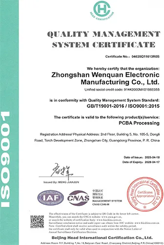
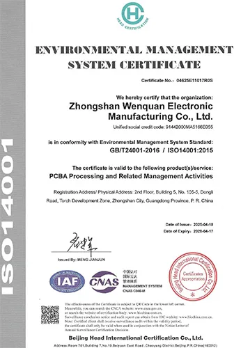
These are management-system certificates, not product or batch COAs. No batch inspection reports or COAs are currently published here.
Frequently asked questions
Questions that shape the pcb design services route
Use these answers to prepare the files, approvals and production handoff before requesting a quote.
What are PCB design services?
PCB design services turn product requirements, schematics or reference data into a manufacturable board package. The scope can include component and stackup planning, layout coordination, DFM/DFA review, revision control and production handoff.
Can PCB design include stackup and material planning?
Yes. Stackup and material planning can be reviewed from layer count, impedance, copper, thermal, flex or rigid-flex and mechanical requirements. The final selection is confirmed against the released design and manufacturing process.
What files are delivered after a PCB design service?
The delivery package is project-specific, but can include approved source data, Gerber or ODB++, NC drill, stackup, fabrication drawing, assembly drawing, BOM, pick-and-place data and revision notes.
Does PCB design service include PCB manufacturing and assembly?
Design support can be connected to PCB manufacturing and assembly through DFM/DFA review and a controlled handoff. Fabrication, component sourcing and assembly are quoted as separate production scopes unless the project package defines a combined turnkey route.
Related pages
Connect engineering work to the next production decision.
Keep the design, layout, fabrication, assembly and validation route connected through the existing PCBArise pages.
PCB Manufacturing
PCB Layout Services
Placement, routing, impedance and manufacturing-ready layout support.PCB ManufacturingDFM Review
Manufacturing and assembly checks before production release.PCB ManufacturingPCB Manufacturing Capabilities
Fabrication limits for layers, copper, drills and impedance.PCB ManufacturingPCB Materials & Stackup
Material and stackup decisions for electrical and mechanical fit.PCB ManufacturingTurnkey PCB Assembly
Connect the released design to sourcing, assembly and testing.Ready to review pcb design services?
Share the available design files, requirements and target build with the PCBArise engineering team.