
Uniform heavy copper
Use one heavier finished copper target where power routing dominates most of the board.
Heavy copper PCB manufacturing supports higher-current circuits through controlled copper weight, current density, reinforced vias and thermal design.
Copper thickness, conductor width, temperature rise, via transfer and terminal geometry must be solved together. More copper does not repair a narrow or poorly connected current path.
Use one heavier finished copper target where power routing dominates most of the board.
Combine wide heavy-current areas with finer control routing after etch and spacing rules are reviewed.
Use via arrays and plated structures sized for current transfer, thermal load and manufacturing aspect ratio.
Concentrate additional copper only where the qualified process and design geometry justify it.
Etch geometry changes as copper gets thicker. Minimum line and space, annular ring and finished hole requirements must be evaluated against the selected copper weight.
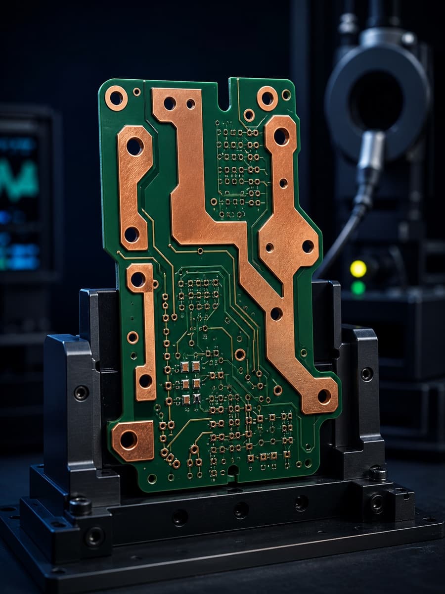
Power-board construction reference
| Finished copper weight | 3–12 oz |
|---|---|
| Layer construction | Single-sided, double-sided or multilayer by review |
| Base materials | FR-4, High-Tg and application-specific power laminates |
| Trace / spacing | Defined by copper weight, conductor profile and finished tolerance |
| Via structures | Reinforced plated through-holes and current-transfer via arrays |
| Board thickness | Selected from current, mechanical and aspect-ratio requirements |
| Surface finish | ENIG, OSP or lead-free HASL as the assembly requires |
| Thermal features | Copper spreading, thermal vias and mechanical heat interfaces |
| Testing | Electrical test plus dimensional and cross-section review as specified |
Capability values are design-dependent. Material, copper weight, layer count, via structure, finished thickness and surface finish can change the achievable combination.
Heavy copper increases etch compensation and changes how closely fine features can be placed. The layout should separate high-current conductors from control routing instead of forcing one geometry across the board.
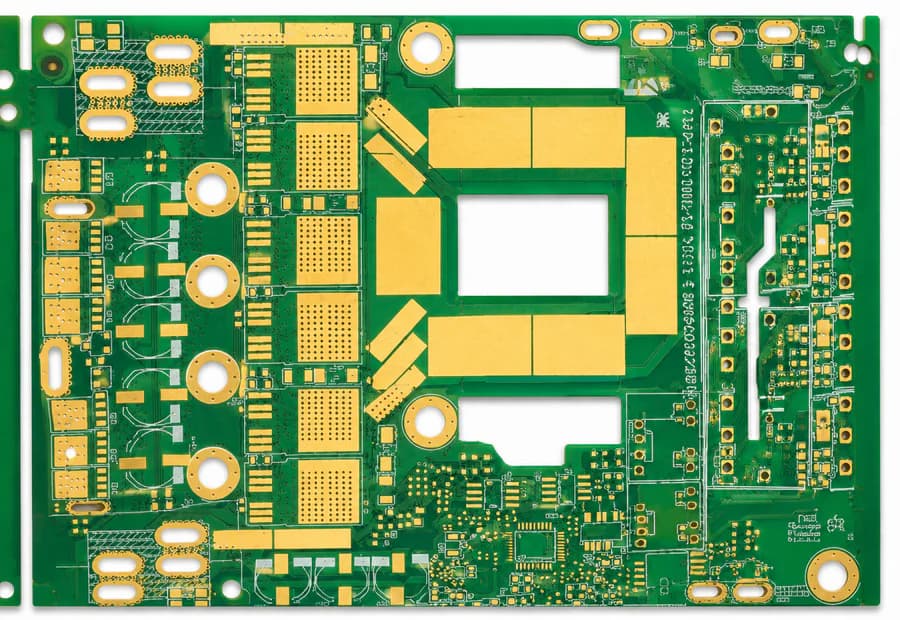
Review finished copper, conductor geometry, reinforced vias, resin flow and thermal behavior as one heavy copper system.
Use these examples as a starting point. The board construction still follows the product’s electrical, mechanical and qualification requirements.
Bus structures, protection boards and high-current distribution inside equipment.
Motor control, inverters and switching stages with repeated current demand.
Battery management, charging and protection circuits with power and control sections.
Converters, storage interfaces and power-conditioning electronics.
Power control, charging and high-current auxiliary systems.
Equipment with concentrated current paths and robust terminal requirements.
Quality documents
The published ISO records name Zhongshan Wenquan Electronic Manufacturing Co., Ltd. and its Zhongshan PCBA facility. They do not certify every PCBArise facility, service or product.
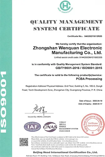
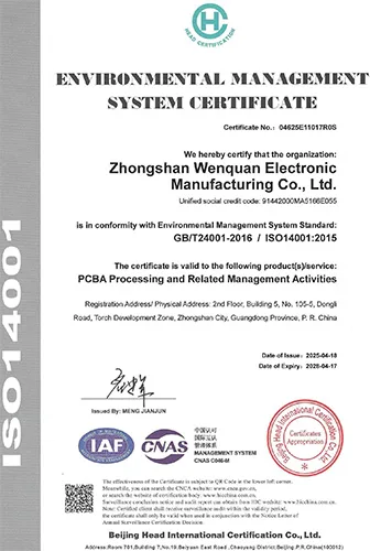
These are management-system certificates, not product or batch COAs. No batch inspection reports or COAs are currently published here.
These answers address copper weight, spacing, current transfer and manufacturing review for power PCBs.
A heavy copper PCB commonly uses finished copper from 3 oz upward. This page covers the published 3–12 oz range, with final geometry confirmed from the complete stackup and current requirements.
Yes, but the layout and fabrication route must account for different etch behavior. Power and control areas should be separated and reviewed rather than assuming standard fine-line rules apply everywhere.
Heavier copper increases conductor cross-section, but current capacity still depends on trace width, connection points, vias, duty cycle, cooling and allowable temperature rise.
Choose heavy copper when current carrying and robust power interconnection are the primary constraints. Choose metal core when moving heat into a chassis or heatsink is the main job. Some designs require both considerations.
Compare heavy copper with metal core, rigid FR-4, capability limits and DFM review before release.
Share the available Gerber, ODB++, drawing, stackup or project requirements with the PCBArise team.