
Industrial IoT sensor PCB for temperature, pressure, vibration, energy and condition monitoring
Industries / PCB & PCBA
IoT Sensor & Smart Gateway PCB Manufacturer
PCBArise manufactures IoT sensor PCB and PCBA for smart gateways, Wi-Fi/BLE/Zigbee/Thread modules, industrial IoT nodes, wearables, asset trackers and smart-home products. The board is judged by the connected product it must fit: antenna performance, battery life, sensor accuracy, enclosure, wireless module package and the path from engineering sample to repeat production.
HDI 1+N+1 to 4+N+4±5% Tight Impedance01005 PlacementPrototype to Production
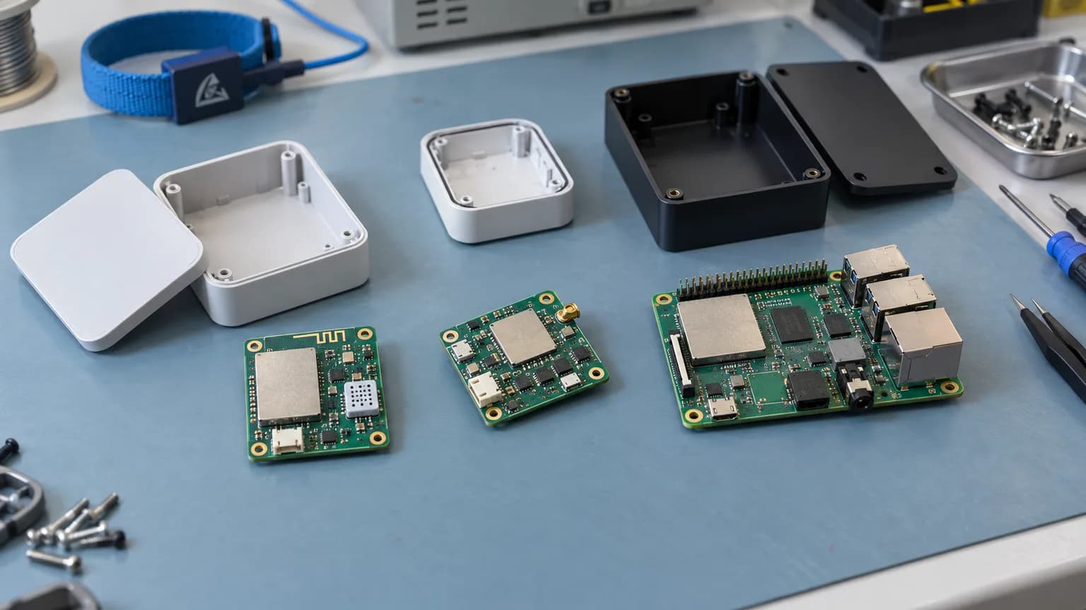
Product useIoT Sensor, Wireless Module & Smart Gateway ApplicationsChosen for your product
Board constructionCompact IoT Gateway and Sensor PCB Construction
Assembly routeIoT PCBA for Wireless Modules, Sensors & Wearables
Quality checksIoT Product Quality, RF & Functional Evidence
Typical applications
IoT Sensor, Wireless Module & Smart Gateway Applications
IoT buyers search for a PCB supplier that understands the device category, not only the layer count. We map the board to the gateway, sensor, wearable, tracker or smart-home product before selecting the construction.
Smart gateway, hub and edge-computing boards for Wi-Fi, BLE, Zigbee, Thread and LoRa
Smart-home controls: thermostats, switches, locks, door sensors, cameras and appliances
Wearable, portable and battery-powered electronics using FPC or rigid-flex
Asset tracking, GPS and cellular IoT (NB-IoT/LTE-M) devices
Smart-meter, environmental sensor and connected-energy monitoring boards
Wireless audio, access-control and compact connected accessories
Engineering choices
What IoT Product Teams Need From a PCB Supplier
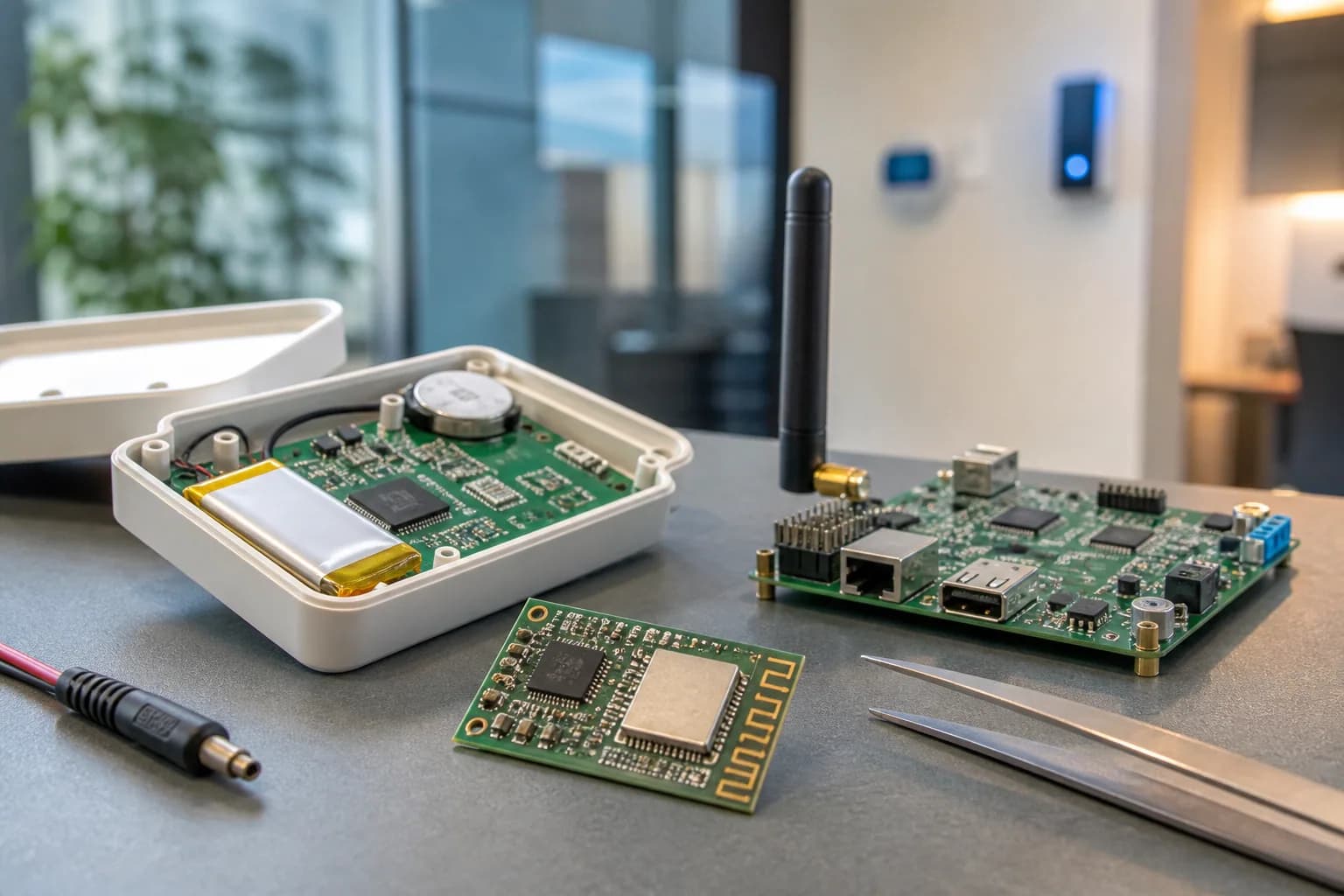
IoT hardware is a product and a radio at the same time. The enclosure, antenna, battery, sensor and wireless SoC create a narrow margin; the supplier must preserve that intent from prototype through the ramp.
Enclosure and antenna: outline, keepout, ground stitching and connector position are part of RF function
Wireless SoC package: fine-pitch BGA/QFN fanout, via-in-pad and HDI affect both size and yield
Sensor integrity: low-level analog, power conversion and digital radio sections need deliberate return paths
Battery life: leakage, cleanliness, coating and sleep-current test can matter more than nominal board size
Product lifecycle: component availability, approved alternates and firmware/programming access support the ramp
Prototype-to-production: the construction and assembly route should reflect the volume product before the enclosure is frozen
Board and process options
Compact IoT Gateway and Sensor PCB Construction
When the gateway or sensor enclosure fixes the board size, HDI, microvias, via-in-pad and controlled impedance become product decisions. The released wireless module, antenna feed and component package determine the final stackup.
Product focus
Connected products need compact construction without losing production access.
Wireless, sensor and smart-home electronics often combine HDI, RF keepouts, small packages, battery power and constrained mechanical envelopes.
- Wireless and antenna keepouts
- HDI, FPC and rigid-flex options
- Battery, connector and test access
Advanced Multilayer & HDI PCB
R&D prototyping and high-end HDI builds
| Parameter | Specification |
|---|---|
| Layer Count | Up to 64 Layers(Prototype / engineering builds) |
| Min Trace Width / Spacing | 2 / 2 mil (0.05 / 0.05 mm) |
| Standard Mechanical Drill | 0.15 mm |
| Advanced / Special Hole Capability | Down to 0.10 mm, subject to design and process review |
| Min Laser Microvia | 0.075 mm |
| Aspect Ratio | Up to 20:1 for qualified designs; 15:1 or below for standard advanced production |
| Controlled Impedance | ±10% standard; ±5% for tighter requirements |
| HDI Structures | 1+N+1, 2+N+2, multi-step HDI and Any-Layer HDI |
| Via Technology | Blind vias, buried vias, stacked vias, staggered vias, via-in-pad, VIPPO / POFV, resin-filled and plated-over vias |
| Sequential Lamination | Supported |
| Any-Layer Interconnection | Supported |
| Back Drilling | Supported |
| Warpage Control | ≤0.5% available when specified, subject to stack-up and design review |
| High-Speed / High-Frequency Materials | Rogers, Taconic/AGC, PTFE/Teflon, F4B, High-Tg FR-4 and other low-loss specialty laminates |
| Board Thickness Tolerance | ±0.05 mm |
| Thermal Conductivity | Up to 3.0 W/m·K(Aluminum PCB) |
Board and process options
Wearable, Sensor & Smart-Home FPC / Rigid-Flex
Wearables, hinges, compact sensors and curved smart-home enclosures may need FPC or rigid-flex to place the radio, battery and display without extra connectors. Bend radius, stiffeners, coverlay and assembly constraints are reviewed by product use case.
Product focus
Connected products need compact construction without losing production access.
Wireless, sensor and smart-home electronics often combine HDI, RF keepouts, small packages, battery power and constrained mechanical envelopes.
- Wireless and antenna keepouts
- HDI, FPC and rigid-flex options
- Battery, connector and test access
FPC / Rigid-Flex PCB Specifications
| Parameter | Specification |
|---|---|
| Layer Count | 1–12 Layers |
| Flexible Material | PI (Kapton), PET, LCP(Rigid area: High-Tg FR-4) |
| Flexible Area Thickness | 0.1–0.6 mm |
| Rigid-Flex Overall Thickness | Up to 3.2 mm |
| Copper Weight | 1/3–2 oz |
| Min Trace Width / Spacing | 3 / 3 mil standard(Advanced: 2 / 2 mil) |
| Dynamic Flexing | Qualification depends on bend radius, copper and stackup |
| Supported Features | Coverlay, Stiffeners, ZIF Connectors, Shielding Layers, Surface Mount Components |
| Testing | 100% Electrical Testing, AOI Inspection, Dynamic Flex Testing, Custom Testing |
Assembly considerations
Materials for Wireless, Sensor & Wearable Products
RF laminate, flex material, finish and shielding are selected for the wireless module, antenna feed, sensor environment and enclosure—not as a generic technology list. The approved stackup and volume target control the final choice.
Options to discuss
Start with what your design needs.
We can confirm the workable combination after reviewing your files.
FR-4High-Tg TG170RogersTaconicPILCPENIGENEPIGImmersion GoldOSPImmersion SilverVia-in-Pad
What to send
Choose for the product you are building.
- Wireless and antenna keepouts
- HDI, FPC and rigid-flex options
- Battery, connector and test access
Board and process options
IoT PCBA for Wireless Modules, Sensors & Wearables
IoT PCBA is small and dense: wireless SoCs, sensors, antenna connectors, shields, batteries and fine-pitch passives often share one assembly. The route covers rigid, FPC and rigid-flex substrates with programming, inspection and functional checks matched to the connected product.
Product focus
Connected products need compact construction without losing production access.
Wireless, sensor and smart-home electronics often combine HDI, RF keepouts, small packages, battery power and constrained mechanical envelopes.
- Wireless and antenna keepouts
- HDI, FPC and rigid-flex options
- Battery, connector and test access
PCB Assembly Specifications
SMT, THT and mixed technology assembly capabilities
| Parameter | Specification |
|---|---|
| Min Component Size | 01005 (0.4 × 0.2 mm) |
| Component Size Range | 01005 to 150 × 100 × 30 mm |
| Min BGA Pitch | 0.25 mm |
| Min QFP / QFN Pitch | 0.15 mm spacing / 0.3 mm width |
| Placement Accuracy (X/Y) | ±0.025 mm (±25 μm) |
| Placement Accuracy (θ) | ±0.2° |
| Max BGA Component Size | 70 × 74 mm |
| Max PCB Assembly Size | 400 × 1200 mm(Min 50 × 50 mm; applicable process-line envelope, subject to board support and panelization review) |
| PCB Thickness Range | 0.3–10.0 mm |
| Warpage Control | ≤0.5%(Subject to board construction and assembly process review) |
| Max Component Height | 120 mm(Applicable equipment and assembly route; confirm package clearance during engineering review) |
| Soldering Methods | Wave Soldering, Selective Soldering, Hand Soldering |
| Reflow Atmosphere | Air / Nitrogen(Nitrogen reflow on applicable lines; oxygen target depends on the assembly route and profile) |
| SMT Production Capacity | 700+ million points / month(Combined figure across 20+ SMT lines; not a per-facility or per-line guarantee) |
Assembly considerations
Prototype-to-Production for Connected Products
The useful prototype is the one that teaches the production build: antenna and sensor performance, programming, test access, BOM risk and assembly yield. Prototype and production quantities are assessed from the released package; the final schedule depends on HDI complexity, process route and component availability.
- Prototype review for enclosure, antenna, sensor placement, programming and test access
- BOM and wireless-module sourcing review with qualified alternates where the project allows
- IC programming, firmware loading and pairing checks when included in the release package
- Conformal coating, box build and final packaging for the finished connected product
- Traceability and repeat-lot records carried into the production ramp
What to send
Choose for the product you are building.
- Wireless and antenna keepouts
- HDI, FPC and rigid-flex options
- Battery, connector and test access
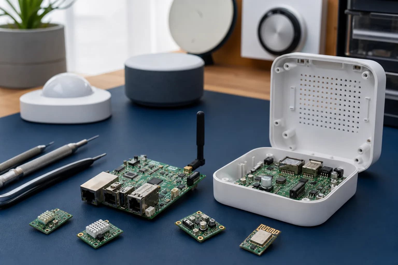
How the board fits the product
Connected products need compact construction without losing production access.
Wireless, sensor and smart-home electronics often combine HDI, RF keepouts, small packages, battery power and constrained mechanical envelopes.
- Wireless and antenna keepouts
- HDI, FPC and rigid-flex options
- Battery, connector and test access
HDI 1+N+1 to 4+N+4±5% Tight Impedance01005 PlacementPrototype to Production
Inspection, testing and records
IoT Product Quality, RF & Functional Evidence
The evidence plan follows the connected product: HDI and assembly inspection, RF or impedance inputs, programming records, electrical coverage, sensor or gateway functional checks and the traceability required for the release. IPC-A-600/A-610 class, coating and acceptance are confirmed from the project files.
ISO 9001:2015ISO 14001:2015
Build files
Keep the board revision, BOM and assembly drawings together so the factory builds the intended configuration.
Inspection and test
Choose optical, X-ray, electrical or functional checks for the defects that matter to this product.
Material tracking
Agree which material and production records you need to retrieve after shipment.
Design changes
Decide who can approve a material, component or process change before it reaches the line.
Quality documents
Preview & download certificates
The published ISO records name Zhongshan Wenquan Electronic Manufacturing Co., Ltd. and its Zhongshan PCBA facility. They do not certify every PCBArise facility, service or product.
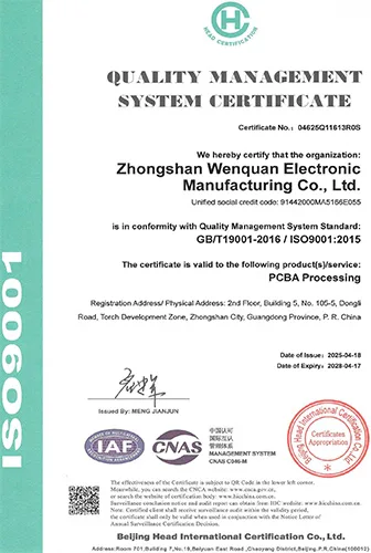
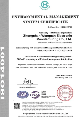
These are management-system certificates, not product or batch COAs. No batch inspection reports or COAs are currently published here.
Frequently asked questions
Common questions about this PCB application
Start with the board, environment and files you have; the detailed route depends on your design.
What HDI structures do you support for compact IoT boards?
We build 1+N+1 through 4+N+4, plus any-layer interconnection, with stacked or staggered vias and via-in-pad. Minimum laser microvia is 0.075 mm; advanced and special-hole capability reaches down to 0.10 mm, with qualified aspect ratio up to 20:1. Volume production covers 1–40 layers; prototype and engineering builds can support up to 64 layers.
What impedance tolerance can you hold on RF and antenna sections?
Standard impedance control is ±10%; ±5% is available for tighter requirements on HDI and RF builds, with board thickness tolerance of ±0.05 mm. Because antenna tuning follows the dielectric stackup, we provide the stackup and impedance calculation during engineering review and hold it consistent across lots.
Do you build flexible and rigid-flex boards for wearables?
FPC and rigid-flex options include PI, PET or LCP, with coverlay, stiffeners, ZIF contacts and assembled components where the design allows. For a moving hinge or wearable, provide the bend radius and target cycle life so the stackup and test plan can be reviewed for that product.
Can you review both prototype and production IoT quantities?
Yes. We review the available prototype or production package, enclosure, wireless module, BOM and target quantity, then confirm the practical PCB and PCBA route. Schedule depends on the released files, HDI or flex complexity, process requirements and component availability rather than a blanket delivery promise.
What is the smallest component and finest pitch you can place?
The published PCBA envelope includes 01005 (0.4 × 0.2 mm), 0.25 mm minimum BGA pitch, QFP/QFN down to 0.15 mm spacing and 0.3 mm width, with ±0.025 mm (±25 μm) X/Y placement accuracy and ±0.2° in θ. Package fit, PoP feasibility, line assignment and inspection coverage are confirmed against the released IoT build.
Will my prototype and my production units be built the same way?
The review targets a production-relevant route early. Prototype and production lines or process settings can differ with quantity, schedule, facility and package mix; the released data, approved materials, process controls and acceptance records are carried forward where the project plan requires them.
Related PCB pages
Explore the board and assembly options behind this product.
Use the related PCB, PCBA and quality pages to plan the next part of your build.
PCBArise resource
HDI PCB
Microvia and any-layer HDI for compact, high-density products.
PCBArise resourceFlexible PCB
FPC and rigid-flex for wearables and space-constrained designs.
PCBArise resourcePCB Prototype
Prototype review and production-aware builds for compact connected devices.
PCBArise resourcePrototype PCB Assembly
Low-volume assembly that scales to mass production without redesign.
PCBArise resourceSMT Assembly
01005 and fine-pitch placement on 20+ SMT lines.
Move the connected product from prototype to repeatable build.
Share the enclosure, wireless, battery and quantity targets so the PCB and PCBA route can be reviewed together.