
Single-sided FPC
One copper layer with the tightest bend radius and lowest construction cost.
Flexible PCB manufacturing treats the circuit as both an electrical interconnect and a mechanical part, with bend radius, cycle life, copper and assembly space designed together.
A flex-to-install interconnect and a lifetime hinge are different products. Bend radius, flex cycles and the rigid transition must be defined early.
One copper layer with the tightest bend radius and lowest construction cost.
Plated through-holes and routing on both sides for mainstream interconnects.
Up to 12 layers where flex routing and controlled impedance must coexist.
Flexible layers laminated into High-Tg FR-4 rigid sections to reduce connectors.
Mechanical use conditions affect every value in the table. Provide the bend radius, flex zone and expected cycle count with the RFQ.
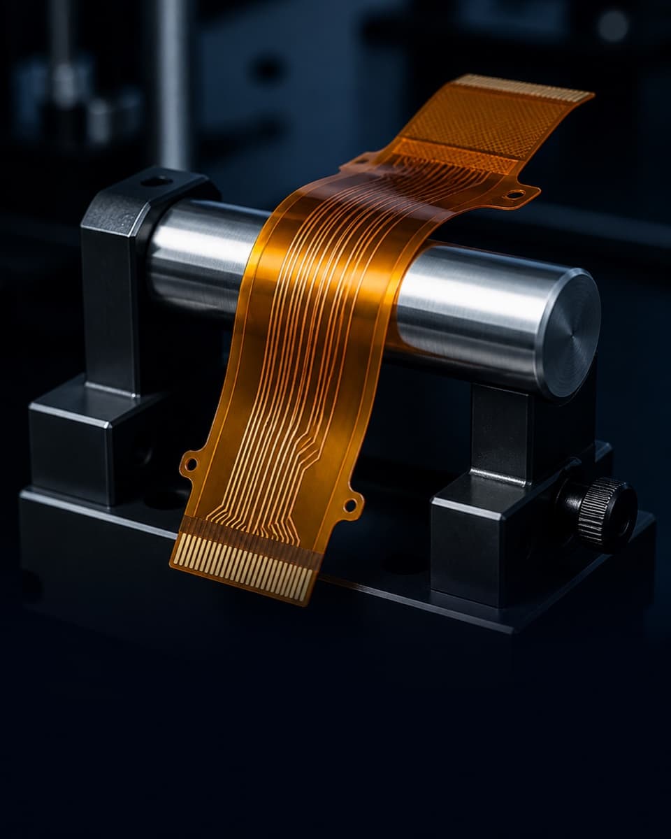
Electrical and mechanical build capability
| Layer count | 1–12 layers |
|---|---|
| Flexible materials | PI (Kapton), PET, LCP; High-Tg FR-4 in rigid areas |
| Flexible area thickness | 0.1–0.6 mm |
| Rigid-flex overall thickness | Up to 3.2 mm |
| Copper weight | 1/3–2 oz |
| Minimum trace / spacing | 3 / 3 mil standard; 2 / 2 mil advanced |
| Dynamic flexing | Defined by bend radius, copper, stackup and qualification plan |
| Supported features | Coverlay, stiffeners, ZIF contacts, shielding layers, SMT |
| Testing | Electrical, AOI, dynamic flex and custom testing as specified |
Capability values are design-dependent. Material, copper weight, layer count, via structure, finished thickness and surface finish can change the achievable combination.
Dynamic flex uses thinner copper and a controlled bend geometry. Plated holes, abrupt trace-width changes and stiffener edges should stay away from the active flex zone.
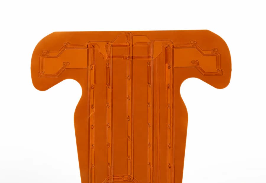
Validate bend radius, trace direction, plated-hole keepouts, stiffener transitions and assembly support against the flex duty.
Use these examples as a starting point. The board construction still follows the product’s electrical, mechanical and qualification requirements.
Folded assemblies with tight space and weight limits.
Hinges, sliders and compact connection paths.
Probes, portable diagnostics and shaped interconnects.
Instrument clusters, cameras and sensor interconnects.
Continuous-motion applications requiring dynamic flex review.
Harness reduction where weight and packaging matter.
Quality documents
The published ISO records name Zhongshan Wenquan Electronic Manufacturing Co., Ltd. and its Zhongshan PCBA facility. They do not certify every PCBArise facility, service or product.
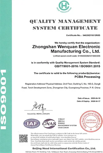
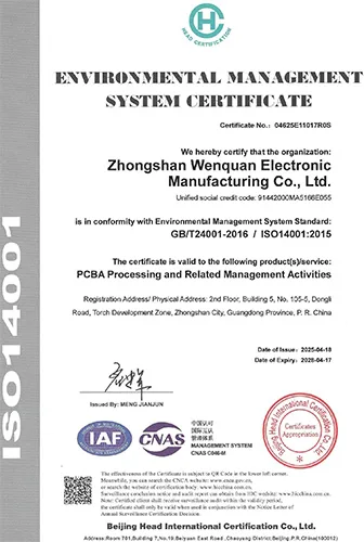
These are management-system certificates, not product or batch COAs. No batch inspection reports or COAs are currently published here.
Use these answers to prepare the mechanical and fabrication information required for flexible PCB review.
Flexible and rigid-flex constructions support 1–12 layers. Most moving flex zones remain lower layer count to preserve bend performance.
Cycle life is defined from the bend radius, copper weight, layer count, trace direction and mechanical envelope, then confirmed through the agreed qualification plan.
The standard flex process window is 3/3 mil. Advanced 2/2 mil geometry is available after material and flex-duty review.
Yes. Component areas normally use stiffeners and dedicated assembly carriers. Placement, support and bend transitions are checked during DFM review.
Compare flexible PCB with rigid, HDI and rigid-flex routes before fixing the mechanical package.
Share the available Gerber, ODB++, drawing, stackup or project requirements with the PCBArise team.