
Component placement around function, connector access, thermal paths and assembly constraints
PCB Manufacturing / engineering service
PCB Layout Services
PCB layout services turn the approved circuit intent into a manufacturable physical design. Placement, high-speed routing, power and ground, controlled impedance, RF constraints, HDI or flex construction and DFM review are coordinated before the production files are released.
PlacementComponent access
RoutingHigh-speed and RF
ImpedanceStackup controlled
ReleaseDFM and fab data
For stackup, layout checks and release files, use the PCB design guide.
Service scope
PCB Layout Service Scope
A PCB layout service should begin with the schematic, netlist and mechanical constraints, then turn the critical electrical and physical decisions into a revision-controlled board layout.
High-speed routing for differential pairs, length matching, return paths and layer transitions
Power and ground layout with current paths, plane strategy and isolation requirements reviewed
Controlled-impedance routing connected to the selected stackup, laminate and copper geometry
RF, HDI, flex and rigid-flex layout decisions reviewed against the intended fabrication process
DFM review and manufacturing-ready Gerber, ODB++, NC drill, stackup and drawing handoff
Technical reference
PCB Layout Inputs and Deliverables
The layout schedule depends on the quality of the input package. The following table shows the information that prevents rework between schematic intent, mechanical packaging and the final manufacturing files.
PCB Layout Service Inputs and Deliverables
Coordinate placement, routing and production release
| Layout inputs | Schematic or netlist, component library, board outline, enclosure and placement constraints |
|---|---|
| Placement plan | Functional partitioning, connector access, thermal components, keepouts and service access |
| Routing plan | Power and ground strategy, differential pairs, length rules, return paths and critical nets |
| Controlled impedance | Target impedance, stackup, material, trace geometry and reference-plane assumptions |
| Special technologies | High-speed, RF, HDI, flex, rigid-flex, via-in-pad or back-drilling requirements where applicable |
| Release package | Gerber or ODB++, NC drill, stackup, fabrication and assembly drawings, BOM and revision notes |
Design context
High-Speed, RF and Power Layout Decisions
Layout quality is determined by the relationships between signal, reference plane, material, component, connector and enclosure. The routing rules must be specific enough to verify before the design is released.
- Place connectors, clocks, converters, processors and sensitive analog or RF blocks from the signal path
- Define differential-pair, length, spacing, via-transition and return-path rules before routing critical nets
- Match controlled-impedance targets to the selected stackup and confirm the fabrication tolerance
- Separate noisy power paths from sensitive analog, RF and measurement areas where the product requires it
- Review antenna keepouts, shielding, back drilling, microvias or rigid-flex transitions when applicable
- Run DFM / DFA and test-access review before Gerber, ODB++ and assembly data are released

Engineering review
What the PCB Layout Review Should Close
The layout is ready for release only when critical nets, stackup assumptions, mechanical fit and manufacturing data can be checked together.
Placement and critical component access
High-speed, RF and power routing rules
Controlled impedance and reference planes
HDI, flex or rigid-flex constraints
DFM / DFA, test access and release files
Practical fit
Where PCB Layout Services Fit
Use PCB layout services when an approved circuit needs placement, routing and production files that respect electrical, mechanical and manufacturing constraints.
High-speed and RF boards
Coordinate differential pairs, return paths, impedance, RF transitions and shielding from the released stackup.
Complex product packaging
Resolve connector access, thermal parts, keepouts, flex transitions and enclosure constraints before release.
Manufacturing-ready release
Close DFM/DFA, test access, Gerber, ODB++, NC drill, stackup and drawing requirements in one revision.
Quality documents
Preview & download certificates
The published ISO records name Zhongshan Wenquan Electronic Manufacturing Co., Ltd. and its Zhongshan PCBA facility. They do not certify every PCBArise facility, service or product.
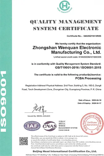

These are management-system certificates, not product or batch COAs. No batch inspection reports or COAs are currently published here.
Frequently asked questions
Questions that shape the pcb layout services route
Use these answers to prepare the files, approvals and production handoff before requesting a quote.
What are PCB layout services?
PCB layout services place components and route the approved circuit on a manufacturable board. The scope can include high-speed, RF, power and controlled-impedance layout, stackup coordination, DFM review and production-file handoff.
Can PCB layout services include high-speed and RF layout?
Yes, when the project provides the required signal, impedance, stackup, connector, shielding and mechanical constraints. RF and high-speed feasibility is confirmed against the released material and fabrication plan.
Do you provide Gerber and ODB++ files after PCB layout?
The project handoff can include Gerber or ODB++, NC drill, stackup, fabrication and assembly drawings, BOM, pick-and-place data and revision notes when those deliverables are included in the approved scope.
How does PCB layout connect to manufacturing?
The layout is reviewed against layer count, material, copper, drill, impedance, assembly and test-access requirements before release. This connects the board layout to PCB fabrication and PCB assembly instead of treating production as a later handoff.
Related pages
Connect engineering work to the next production decision.
Keep the design, layout, fabrication, assembly and validation route connected through the existing PCBArise pages.
PCB Manufacturing
PCB Design Services
Requirements, stackup, DFM/DFA and complete design support.PCB ManufacturingHigh Frequency PCB
RF and microwave material, impedance and via-transition decisions.PCB ManufacturingHDI PCB
Microvia and sequential-lamination layout constraints.PCB ManufacturingRigid-Flex PCB
Mechanical transitions and flexible-area layout considerations.PCB ManufacturingDFM Review
Fabrication and assembly checks before production release.Ready to review pcb layout services?
Share the available design files, requirements and target build with the PCBArise engineering team.