
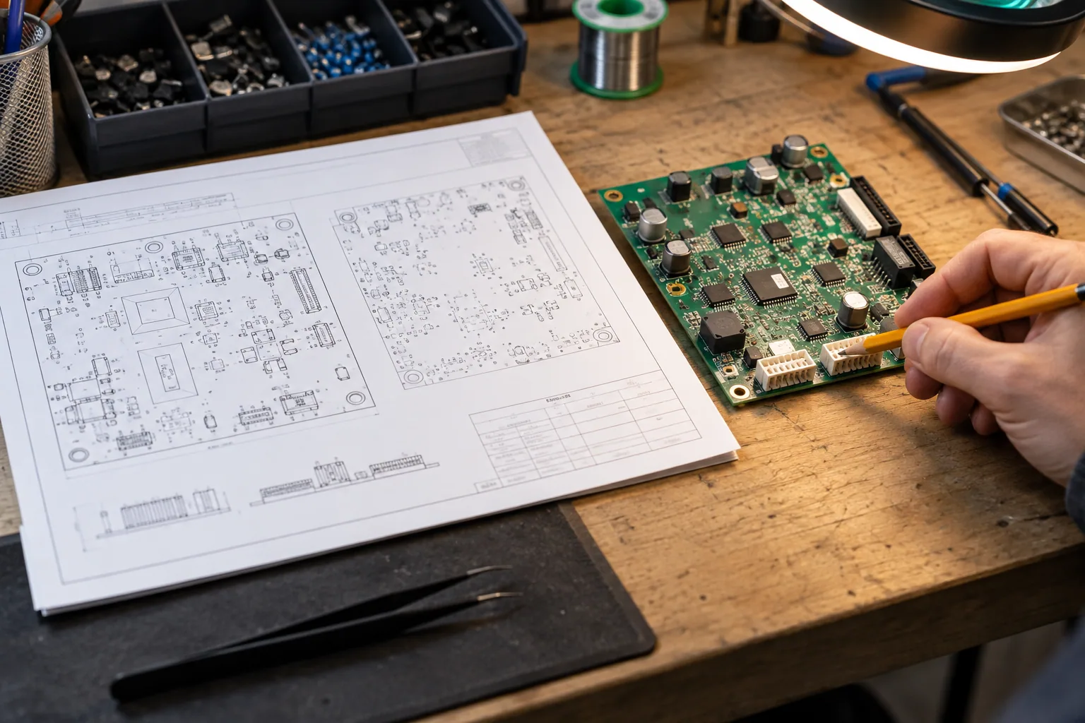
In short
A PCB assembly drawing should answer visual build questions that the BOM and placement file leave open: which side is shown, how polarized parts face, where connectors and hardware sit, and which notes or variants apply. Keep it tied to the same released revision as the CAD, BOM and CPL.
- Show clear top and bottom assembly views with reference designators and a defined viewing convention.
- Mark pin one, polarity and keyed or asymmetric orientation where the footprint alone can be misread.
- Call out DNP, variant, hand-install, hardware and special build notes without duplicating the entire BOM.
- Check the drawing against the BOM and placement data before releasing a single revision-controlled package.
The assembly drawing should answer this: what should the finished board look like? It shows top and bottom component views, readable designators, orientation of polarity-sensitive parts, connector and hardware placement, and only the build notes that are not already clear from the BOM or placement data. Release it with those files under the same revision. If a mark on the board conflicts with the drawing, resolve the difference before assembly.
What the assembly drawing must show
Begin with a board outline, revision, title and units or scale where dimensions are used. Make top and bottom views unmistakable: label the viewing direction and include a recognizable datum such as a mounting hole or keyed connector. Show component outlines and reference designators at a scale that remains legible when printed. Enlarged detail views are better than cramming a fine-pitch area into unreadable labels. Altium’s assembly-documentation guide covers these drawing fundamentals.
The drawing is not a replacement for the fabrication drawing. The latter defines board construction and dimensions; the assembly view explains fitted parts and assembly-specific handling. The IPC documentation-package overview similarly separates drawing purpose from the rest of the product definition.
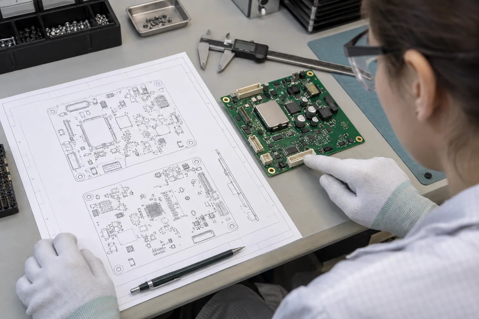
Polarity and orientation: show what a coordinate file cannot
A CPL row can say U7 is rotated 90°, but it does not tell a human whether pin one should face the board corner. For ICs, show a pin-one dot, notch or numbered corner where needed. For diodes and LEDs, show the correct cathode or orientation mark. For electrolytic capacitors, identify the polarity convention used by the actual part and footprint. For keyed connectors, show the mating direction and latch or key side. Eurocircuits’ pin-one and rotation guide illustrates why orientation needs an explicit convention rather than a universal angle assumption.
Use the component manufacturer’s current package drawing when a physical mark could be confused with a mold feature. If the PCB silkscreen is absent, hidden after placement or potentially misleading, the assembly drawing needs an unambiguous detail view. PCBWay’s assembly input guidance also calls for clear polarity and pin-one information.
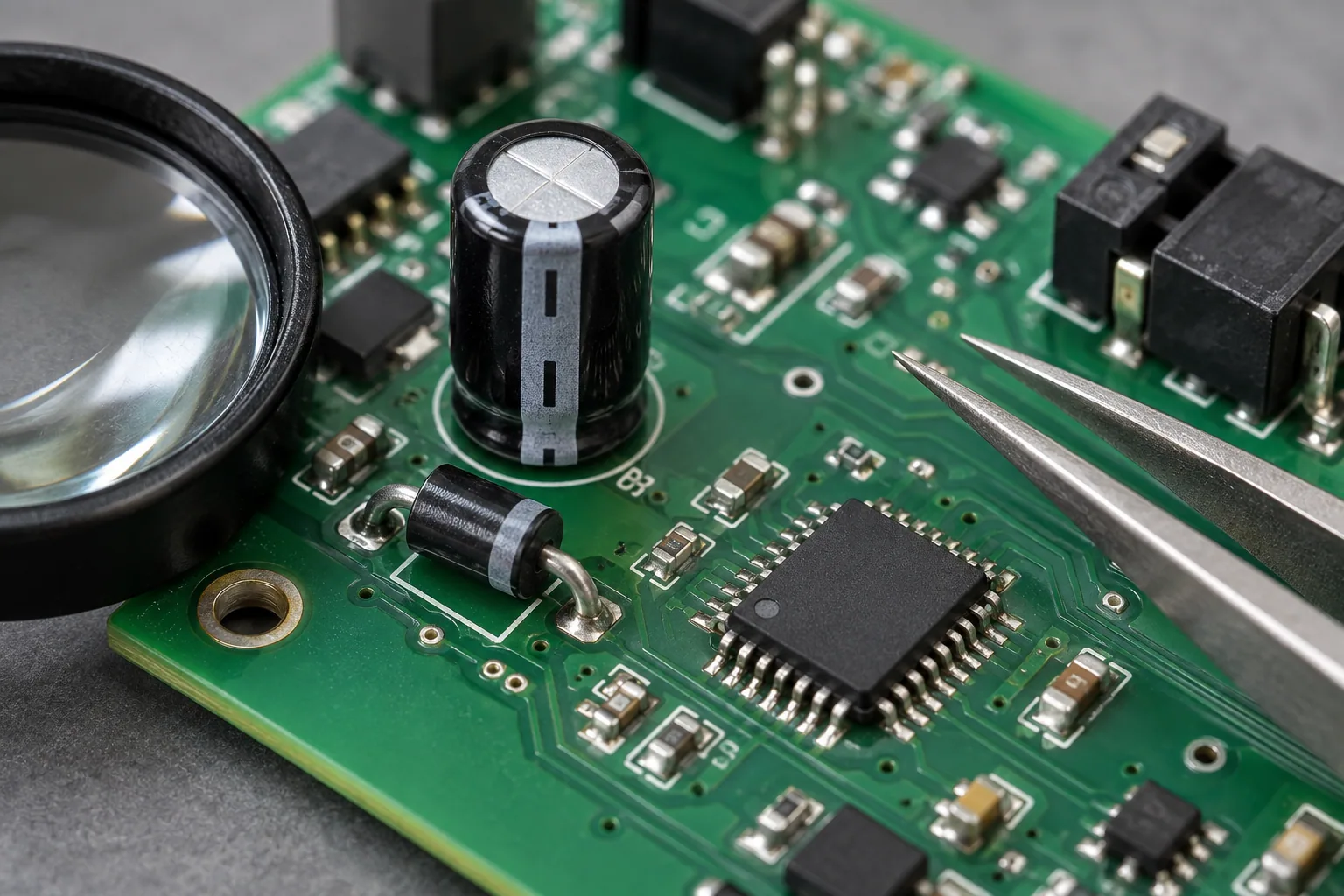
Assembly drawing, BOM and CPL: who owns which answer?
| Buyer question | Primary source | Cross-check |
|---|---|---|
| Which exact component is approved? | BOM and approved alternates | Designator and variant on drawing/CPL |
| Where is it placed? | Pick-and-place/CPL coordinates | Drawing outline and side |
| Which way does it face? | Assembly drawing plus part datasheet | Footprint and machine rotation |
| How is hardware or a hand part installed? | Assembly drawing and build note | BOM and mechanical design |
| Which positions are not fitted? | Variant BOM or controlled fit matrix | Drawing and CPL |
These are complementary outputs, not competing versions of the same instruction. Altium’s assembly-output overview describes the separate roles of BOM, pick-and-place data and drawings. When the three disagree, do not quietly choose whichever seems plausible. Record the discrepancy and issue a corrected, controlled package.
Build notes worth putting on the drawing
Use notes for instructions that change the assembly route or prevent an avoidable interpretation error. Examples include a specifically approved hand-install step, a connector height or seating requirement, mechanical hardware orientation, a keep-clear region for a mating part, a required inspection view, or a variant identifier. State the applicable part or location, not “special handling required” with no subject.
Do not copy a full component table into the drawing if the BOM is the controlled part source. Repeated information goes stale. If an assembly note changes a material, alternate, process or acceptance criterion, identify who approves it and where the controlled decision is recorded. This is particularly important for high connectors, polarized devices and parts installed after reflow.
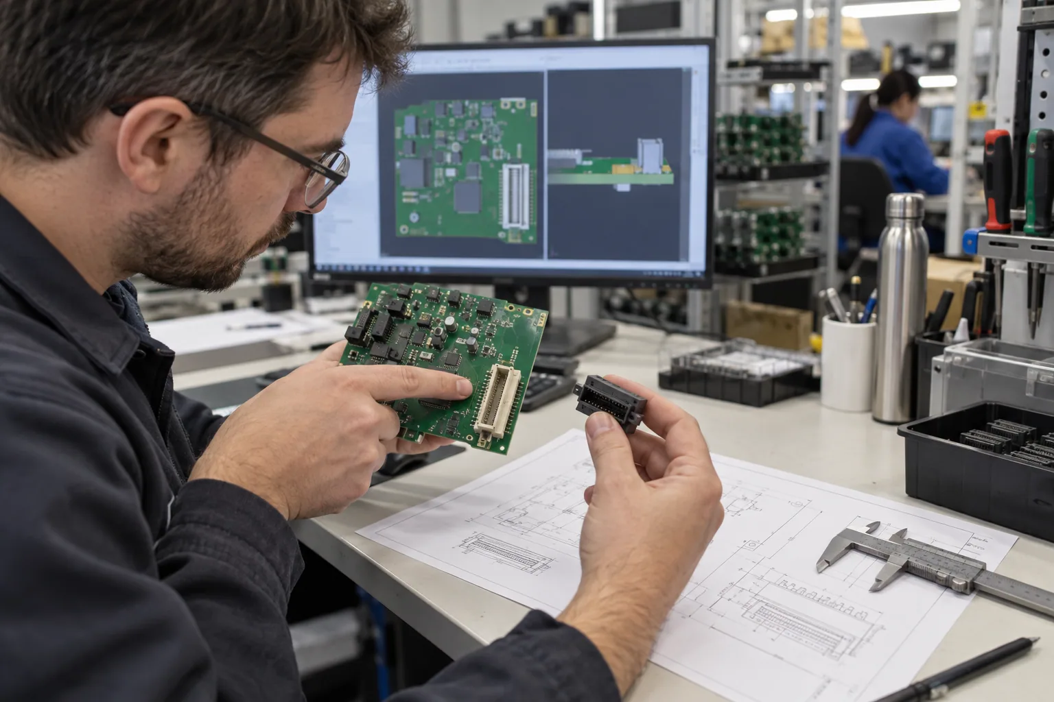
A release flow for a drawing that can actually be built
Before release, print the drawing at the size a production team will use. Can a reader distinguish U7 from U1, see the bottom-side view correctly and find every critical pin-one or polarity mark? Then overlay or compare it with the placement export. A pick-and-place preflight catches coordinate and rotation issues the printed drawing alone may not expose.
Compact checklist for your next handoff
- Same board and variant revision across fabrication data, BOM, CPL and drawing.
- Top and bottom views labeled, with a clear board datum and legible designators.
- Pin one, diode/LED and capacitor polarity, and connector keying shown where relevant.
- DNP and optional positions tied to a controlled fit decision.
- Hand-installed parts, hardware, seating and mechanical clearances called out.
- Any inspection, test or handling instruction tied to a location and acceptance reference.
- Superseded drawings removed from the release package.
When the drawing still leaves an orientation or fit question open, include that question with the current files for a project-specific PCB assembly or DFM review. The point is not to make the document longer; it is to make the build decision visible before parts reach the line.
About the author
PCBArise Electronics
PCBArise Electronics publishes this guide to help design and NPI teams prepare clearer manufacturing files. The requirements for any actual build are confirmed from its current design package.
FAQ
Common questions
Is an assembly drawing required if I already have a BOM and pick-and-place file?+
For a reliable handoff, provide an assembly view or equivalent controlled visual instructions. The BOM identifies parts and the placement file gives coordinates; neither always resolves pin one, connector keying, hardware or special build notes.
What should a PCB assembly drawing include?+
Include labeled top and bottom views, board revision and datum, legible designators, polarity and pin-one marks, keyed orientations, relevant hardware or mechanical details, DNP or variant notes and specific build exceptions.
Should pin one and polarity be marked on both the PCB and drawing?+
Clear PCB marking is helpful, but it may be hidden, crowded or ambiguous. Keep the assembly drawing and part datasheet as controlled references, especially for packages where a mark can be misread.
How should bottom-side components be shown?+
Label the bottom view and state its viewing convention. Use a recognizable datum or keyed feature so a reader can distinguish a true bottom view from a mirrored top view.
Where should DNP information live?+
The variant BOM or controlled fit matrix should own the fit decision. The assembly drawing should flag affected positions visually, and the active placement data must agree.
What if the assembly drawing conflicts with the BOM or CPL?+
Treat the package as unresolved. Confirm the intended revision and variant, correct the source outputs, withdraw superseded files and release one consistent package before assembly.
Technical references
Sources used for this guide
These sources explain the standards, materials or process details discussed above. Check the current revision when applying them to a new design.