
In short
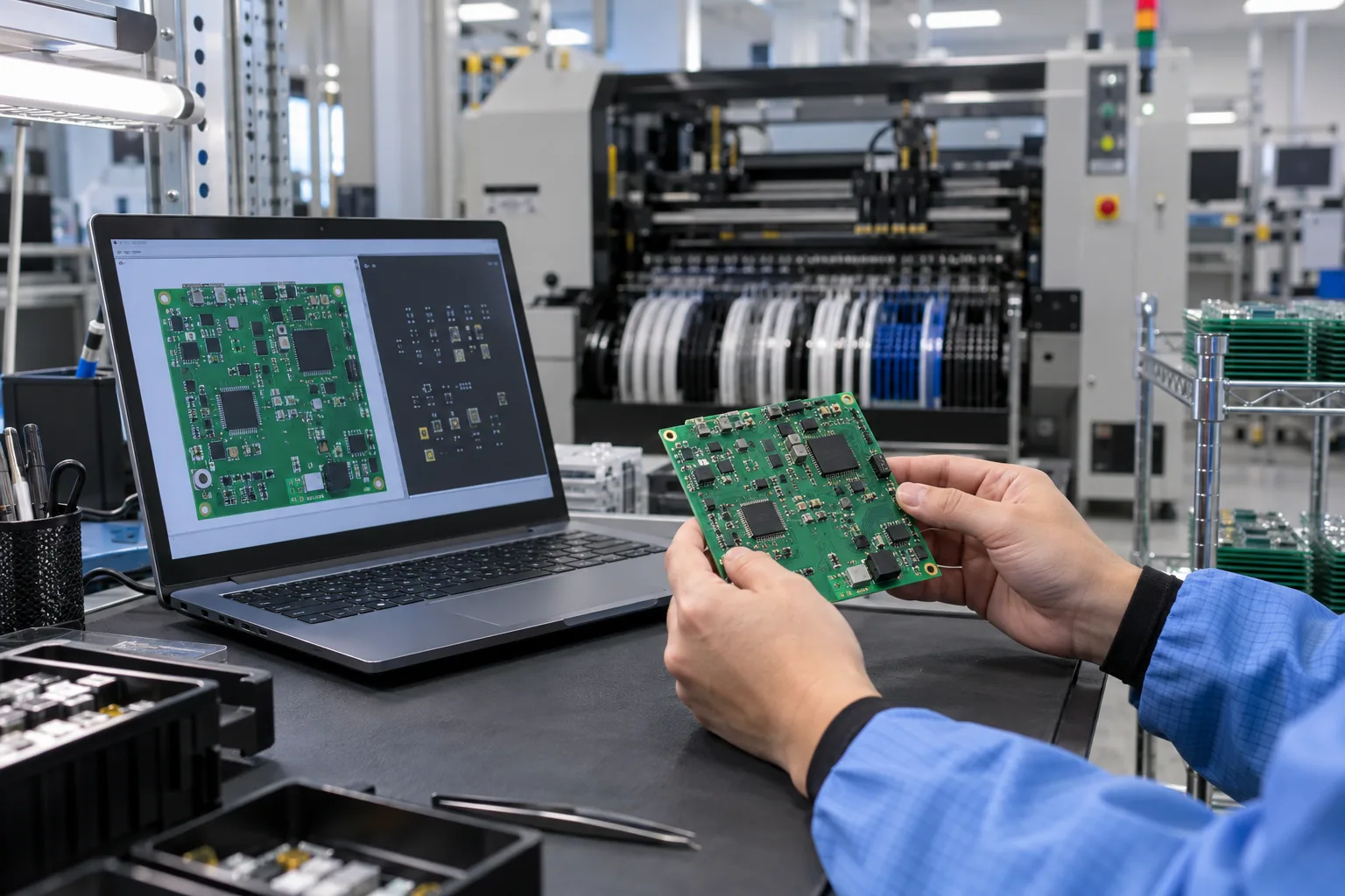
A pick-and-place file should locate every fitted component on the correct board revision, not merely export rows from CAD. Compare it with the BOM and assembly drawing, then confirm the origin and rotation convention with the assembler before machine programming.
- Match every fitted reference designator to the released BOM and drawing; identify do-not-fit positions separately.
- State units, board origin, top/bottom view and rotation convention instead of assuming a machine will infer them.
- Check polarized and asymmetric parts against pin-one or polarity marks on the actual footprint.
- Release one revision-controlled package and resolve exceptions before placement programming.
A usable pick-and-place file tells the assembler which fitted component goes where and how it is oriented on a specific PCB revision. Before handoff, reconcile its reference designators with the BOM, confirm the coordinate origin and units, identify the board side, and inspect rotation on polarized or asymmetric parts. A syntactically valid CSV can still place a connector backwards. That is why the file must be checked alongside the assembly drawing, not in isolation.
What belongs in a pick-and-place file?
Many CAD tools call it a centroid, CPL or component-placement file. A typical row carries a reference designator, center X and Y, board side and rotation. Formats vary by CAD export and assembler; some accept or request footprint and value columns too. JLCPCB’s file guide and Eurocircuits’ CPL guide show why the same basic fields must be interpreted with a known coordinate system.
Do not treat the file as the parts list. The BOM names approved manufacturer parts, quantities and fit status; the placement file names locations. The drawing communicates orientation and build exceptions. A single released revision should make the three agree.
| Field or cross-check | What to confirm | If wrong or missing |
|---|---|---|
| Reference designator | One row per fitted position; spelling matches BOM and drawing | Missing, duplicate or unintended placement |
| X/Y and units | Component center, mm or inches, same origin as board data | All positions offset or scaled |
| Side | Top or bottom with a stated view convention | Mirrored or wrong-side placement |
| Rotation | CAD zero angle and positive direction understood by assembler | IC pin one, diode, LED or connector faces wrong way |
| Revision and fit status | Matches released PCB/BOM; DNP and variants explicit | Machine program built from mixed revisions |
Five errors that turn a clean export into a production question
1. The origin or units changed between files
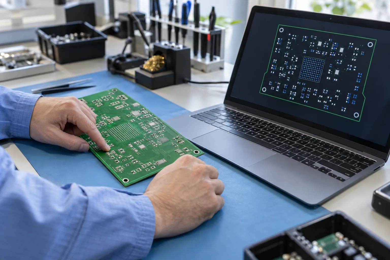
A board can have a CAD origin, a fabrication datum and a panel or machine origin. If the placement export uses one while the assembly setup assumes another, every position can shift. State the file origin, units and whether coordinates describe a single board or panel. Overlay the exported centroids on the current board outline; checking just one component near the center may hide a mirrored or scaled data set.
2. Bottom-side coordinates were mirrored twice—or not at all
Bottom-side views differ by tool. A placement viewer may display the board from the bottom while the CAD export retains top-view coordinates. Label the viewing convention and check a bottom-side connector or unmistakable asymmetric footprint against the assembly drawing. Do not “correct” a whole side by guessing; ask the assembler which transform its import expects.
3. Rotation looked right in CAD but not at the machine
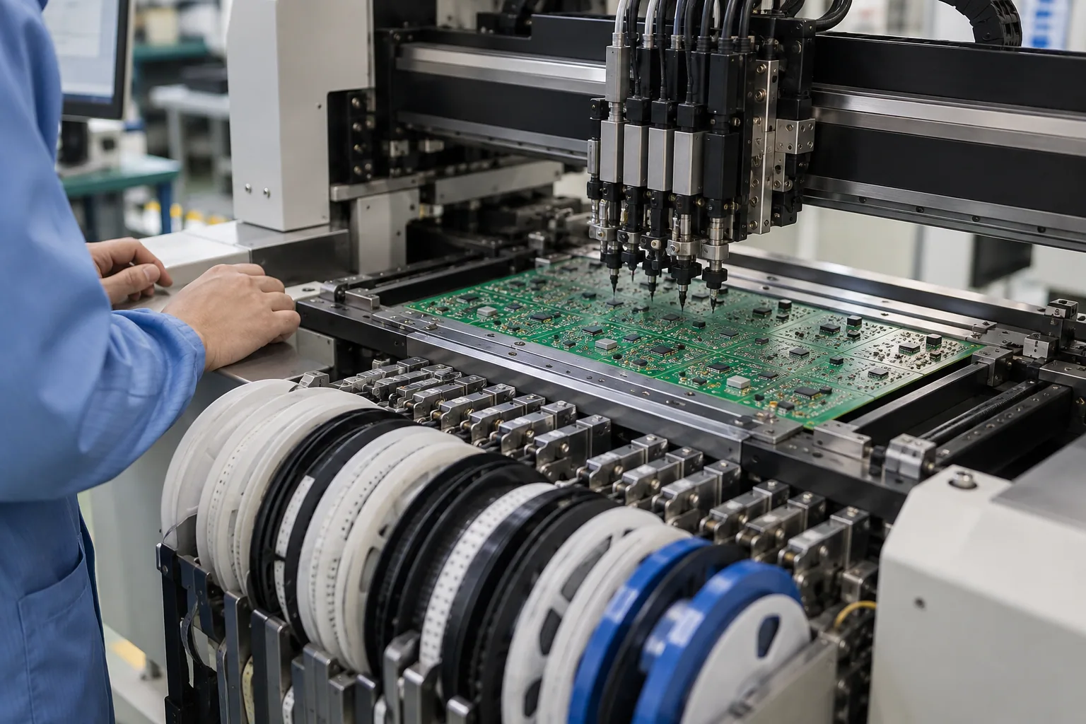
Zero-degree orientation is not universal across libraries, component packages and placement machines. The correct question is not whether a CSV says 90°, but whether the delivered part’s pin one or polarity feature lands at the intended pad. Eurocircuits describes additional machine setup beyond centroid import. Review sample rotations for ICs, diodes, LEDs, electrolytics and keyed connectors; use the manufacturer package drawing when the mark is ambiguous.
4. The BOM, CPL and drawing name different positions
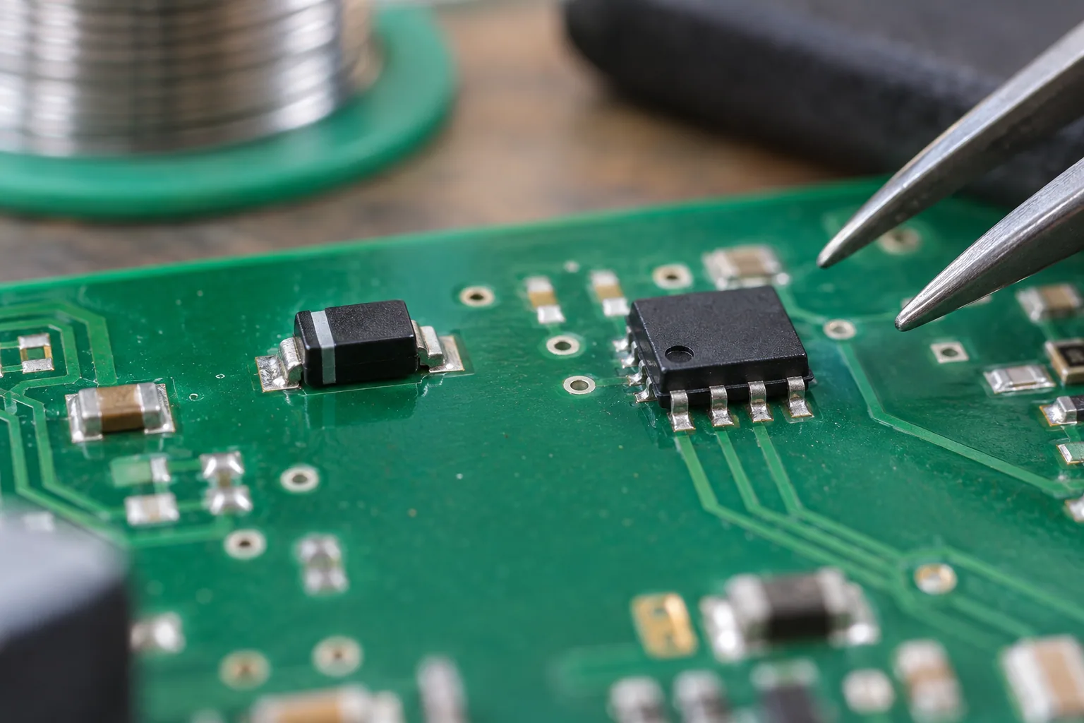
Common causes include late ECOs, refdes renumbering, alternate footprints and a BOM exported from a different variant. For each CPL reference, find exactly one BOM fit decision. For each fitted BOM reference, find one placement row or a documented reason it is hand-placed or otherwise excluded. Make no assumption that a blank BOM cell means “do not fit.” PCBWay’s assembly guidance likewise asks that designators and orientation information be consistent across the package.
5. DNP and variants were left for someone to infer
A single board may support multiple product variants. Give each variant a named BOM and placement-data pair, or a controlled fit matrix that the assembler accepts. State DNP positions explicitly and separate test-only, hand-installed and customer-installed items. Otherwise a row can look like an instruction to populate a footprint that should remain empty.
A preflight flow before sending placement data
For a fast sanity check, export a PDF or viewer image with reference designators and centroids over the board outline. Ask a second person to inspect a sample from each side plus every polarity-sensitive package. This is more useful than relying on a green “import succeeded” message.
Example: find a conflict before the first board
Consider an illustrative, not customer-derived data set: the BOM says U7 is fitted and D4 is DNP; the CPL contains U7 at 42.5 mm, 18.0 mm, top, 90° and also contains D4; the drawing puts U7 pin one toward the board corner. The immediate action is to remove or explicitly exclude D4 for that variant. For U7, compare the footprint’s zero angle, the supplied package’s pin-one mark and the assembler’s rotation convention. Changing 90° to 270° on intuition would create a second uncontrolled error.
If the issue changes design intent, issue a revised export and note the superseded file. If only the assembler’s machine convention differs, retain the design source and document the approved programming transform. Either way, the released package should make the decision reproducible.
What to send with the file
- Gerber or ODB++ and fabrication drawing for the same PCB revision.
- BOM with manufacturer part numbers, fitted quantities, DNP status and variant identifier.
- Top and bottom placement export with units, origin and rotation convention.
- Assembly drawing or marked views showing pin one, polarity and special build notes.
- Any approved deviation or substitution decision, with revision and scope.
If you have the placement data but are still resolving an exception, send the known files for a project-specific DFM and assembly review. For broader PCB assembly scope, include the intended quantity and inspection or test requirements; the engineering discussion can then focus on the actual mismatch rather than a generic file checklist. The related assembly drawing checklist covers the visual instructions that a CPL cannot carry.
About the author
PCBArise Electronics
PCBArise Electronics publishes this guide to help design and NPI teams prepare clearer manufacturing files. The requirements for any actual build are confirmed from its current design package.
FAQ
Common questions
Is a pick-and-place file the same as a BOM?+
No. The BOM identifies approved parts, quantities and fit decisions; the placement file gives locations, board side and rotation for placed references. Reconcile both against the same assembly revision.
Which columns should a PCB assembly placement file contain?+
At minimum, supply reference designator, X/Y center, board side and rotation, plus a clear statement of units and origin. Confirm the preferred import format and any additional footprint or value fields with the assembler.
Should DNP components appear in the pick-and-place file?+
Do not leave that ambiguous. Exclude DNP positions from the active variant file or mark them through an agreed controlled fit matrix, and make the BOM and drawing consistent.
Why can a component rotate incorrectly even when its CAD view is correct?+
CAD libraries, package drawings and placement machines may use different zero-angle and positive-rotation conventions. Check pin one or polarity on representative packages and document the accepted transform.
Do I need separate top- and bottom-side files?+
Some assemblers accept one file with a side column; others prefer separate exports. Either way, identify each side and its view convention, and test asymmetric footprints against the drawing.
What should I do if the BOM and CPL disagree?+
Stop treating the package as released. Identify the correct design and variant revision, resolve the refdes or fit mismatch, regenerate affected outputs and send one clearly named replacement package.
Technical references
Sources used for this guide
These sources explain the standards, materials or process details discussed above. Check the current revision when applying them to a new design.