
Wearables, smartwatches, health and activity trackers with compact sensor boards
Industries / PCB & PCBA
Consumer Electronics PCB & PCBA Manufacturer
PCBArise manufactures consumer electronics PCB and PCBA for wearables, earbuds, smart-home devices, portable products, wireless modules, displays and connected accessories. The board choice follows the product users hold: enclosure, battery, antenna, display, flexing, fine-pitch package, cost target and production ramp are reviewed together.
Compact HDI01005 PlacementFPC & Rigid-FlexPrototype to Production
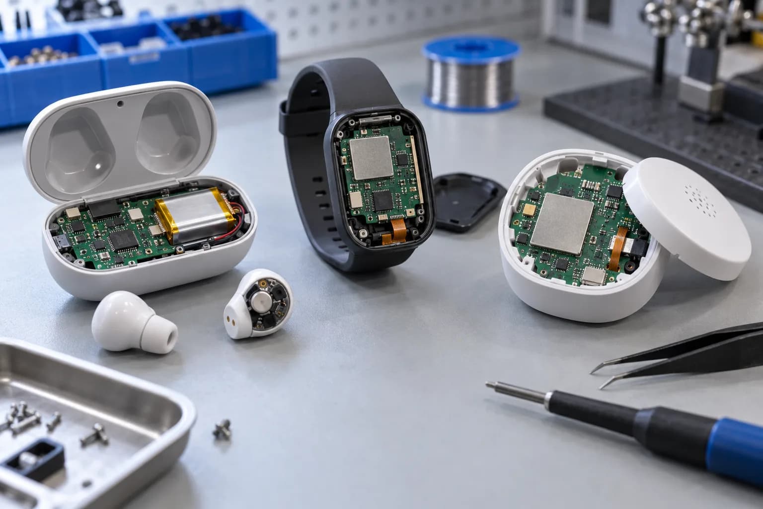
Product useWearable, Smart-Home & Portable Device PCB ApplicationsChosen for your product
Board constructionCompact Wearable & Smart-Device HDI PCB
Assembly routeConsumer PCBA for Wearables, Audio & Smart Home
Quality checksConsumer Product Quality, Test & Production Handoff
Typical applications
Wearable, Smart-Home & Portable Device PCB Applications
Consumer electronics buyers need a PCB supplier that understands the product experience as well as the board. We start with the device category and its mechanical, wireless and battery constraints.
Wireless headphones, earbuds, speakers and portable audio products
Smart-home hubs, displays, cameras, locks, appliances and control panels
Portable consumer devices with battery charging and power-management boards
Wireless modules, sensor nodes and connected accessories
Tablets, handheld controllers and compact display electronics
Engineering choices
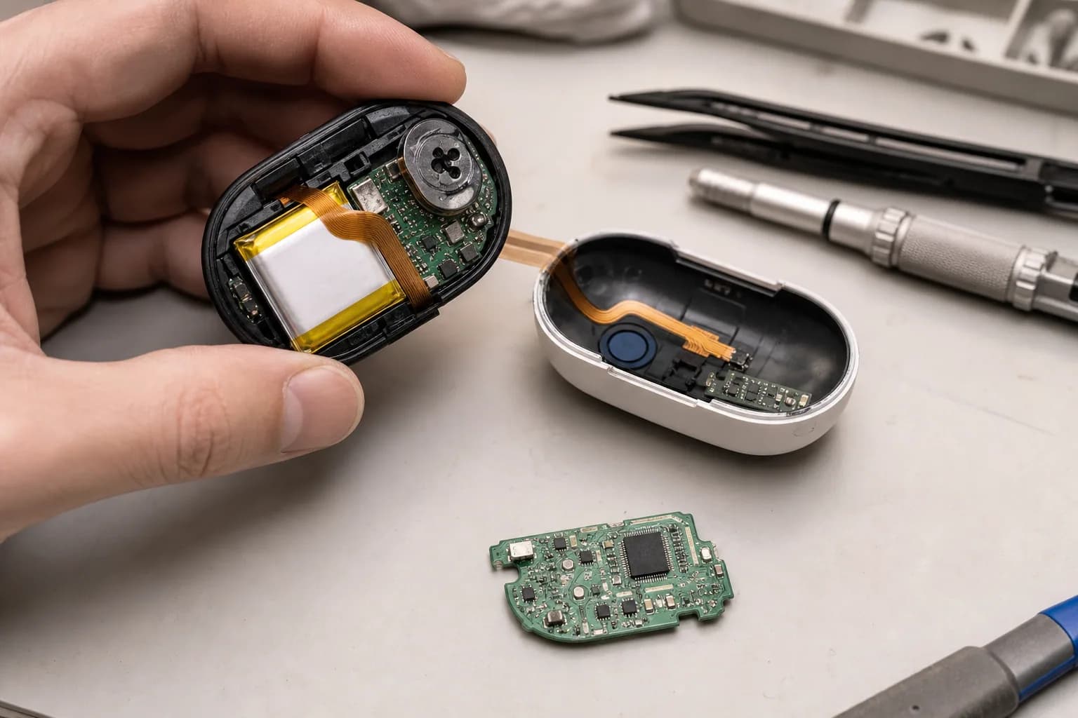
What Consumer Product Teams Need From a PCB Supplier
A consumer PCB is successful when it fits the product, ships on the target schedule and keeps its wireless, battery and cosmetic experience stable at volume. Prototype success alone is not a production handoff.
Wearable and portable enclosures push fine-pitch fanout, HDI, FPC, rigid-flex and connector placement
Wireless and antenna performance depends on stackup, ground reference, keepout and enclosure materials
Battery products need charging control, thermal paths, mechanical retention and low-leakage surfaces
Display, hinge, ZIF and user-facing connector areas need a product-specific workmanship plan
Short product cycles make BOM availability, qualified alternates and change control central to sourcing
Production-relevant prototype construction prevents a second risk during the volume ramp
Board and process options
Compact Wearable & Smart-Device HDI PCB
HDI, controlled impedance, via-in-pad and fine-pitch fanout are evaluated against the wearable, smart-home or portable product envelope and the actual component package.
Product focus
A compact consumer product still needs a production-sized review.
Small enclosures, wireless interfaces, battery limits and cost targets all influence stackup, component sourcing, test access and assembly yield.
- Fine-pitch and HDI fanout
- RF, battery and enclosure constraints
- Prototype learning carried into production
Advanced Multilayer & HDI PCB
R&D prototyping and high-end HDI builds
| Parameter | Specification |
|---|---|
| Layer Count | Up to 64 Layers(Prototype / engineering builds) |
| Min Trace Width / Spacing | 2 / 2 mil (0.05 / 0.05 mm) |
| Standard Mechanical Drill | 0.15 mm |
| Advanced / Special Hole Capability | Down to 0.10 mm, subject to design and process review |
| Min Laser Microvia | 0.075 mm |
| Aspect Ratio | Up to 20:1 for qualified designs; 15:1 or below for standard advanced production |
| Controlled Impedance | ±10% standard; ±5% for tighter requirements |
| HDI Structures | 1+N+1, 2+N+2, multi-step HDI and Any-Layer HDI |
| Via Technology | Blind vias, buried vias, stacked vias, staggered vias, via-in-pad, VIPPO / POFV, resin-filled and plated-over vias |
| Sequential Lamination | Supported |
| Any-Layer Interconnection | Supported |
| Back Drilling | Supported |
| Warpage Control | ≤0.5% available when specified, subject to stack-up and design review |
| High-Speed / High-Frequency Materials | Rogers, Taconic/AGC, PTFE/Teflon, F4B, High-Tg FR-4 and other low-loss specialty laminates |
| Board Thickness Tolerance | ±0.05 mm |
| Thermal Conductivity | Up to 3.0 W/m·K(Aluminum PCB) |
Board and process options
FPC & Rigid-Flex for Wearables and Hinges
FPC and rigid-flex can route around batteries, hinges, displays and curved enclosures while reducing connectors. Bend radius, stiffener, coverlay, dynamic flexing and assembly constraints are confirmed for the product motion.
Product focus
A compact consumer product still needs a production-sized review.
Small enclosures, wireless interfaces, battery limits and cost targets all influence stackup, component sourcing, test access and assembly yield.
- Fine-pitch and HDI fanout
- RF, battery and enclosure constraints
- Prototype learning carried into production
FPC / Rigid-Flex PCB Specifications
| Parameter | Specification |
|---|---|
| Layer Count | 1–12 Layers |
| Flexible Material | PI (Kapton), PET, LCP(Rigid area: High-Tg FR-4) |
| Flexible Area Thickness | 0.1–0.6 mm |
| Rigid-Flex Overall Thickness | Up to 3.2 mm |
| Copper Weight | 1/3–2 oz |
| Min Trace Width / Spacing | 3 / 3 mil standard(Advanced: 2 / 2 mil) |
| Dynamic Flexing | Qualification depends on bend radius, copper and stackup |
| Supported Features | Coverlay, Stiffeners, ZIF Connectors, Shielding Layers, Surface Mount Components |
| Testing | 100% Electrical Testing, AOI Inspection, Dynamic Flex Testing, Custom Testing |
Assembly considerations
Materials for Wireless, Battery & Wearable Electronics
Material and finish follow the product’s RF, thermal, flexing, solderability, appearance and lifecycle requirements—not a generic consumer-electronics recipe.
Options to discuss
Start with what your design needs.
We can confirm the workable combination after reviewing your files.
FR-4High-Tg TG170RogersPILCPAluminumENIGENEPIGOSPImmersion SilverCoverlayVia-in-Pad
What to send
Choose for the product you are building.
- Fine-pitch and HDI fanout
- RF, battery and enclosure constraints
- Prototype learning carried into production
Board and process options
Consumer PCBA for Wearables, Audio & Smart Home
Dense SMT, fine-pitch packages, connectors, shielding, batteries and flex circuits are assembled to the approved BOM, drawings, workmanship and functional requirements of the consumer product.
Product focus
A compact consumer product still needs a production-sized review.
Small enclosures, wireless interfaces, battery limits and cost targets all influence stackup, component sourcing, test access and assembly yield.
- Fine-pitch and HDI fanout
- RF, battery and enclosure constraints
- Prototype learning carried into production
PCB Assembly Specifications
SMT, THT and mixed technology assembly capabilities
| Parameter | Specification |
|---|---|
| Min Component Size | 01005 (0.4 × 0.2 mm) |
| Component Size Range | 01005 to 150 × 100 × 30 mm |
| Min BGA Pitch | 0.25 mm |
| Min QFP / QFN Pitch | 0.15 mm spacing / 0.3 mm width |
| Placement Accuracy (X/Y) | ±0.025 mm (±25 μm) |
| Placement Accuracy (θ) | ±0.2° |
| Max BGA Component Size | 70 × 74 mm |
| Max PCB Assembly Size | 400 × 1200 mm(Min 50 × 50 mm; applicable process-line envelope, subject to board support and panelization review) |
| PCB Thickness Range | 0.3–10.0 mm |
| Warpage Control | ≤0.5%(Subject to board construction and assembly process review) |
| Max Component Height | 120 mm(Applicable equipment and assembly route; confirm package clearance during engineering review) |
| Soldering Methods | Wave Soldering, Selective Soldering, Hand Soldering |
| Reflow Atmosphere | Air / Nitrogen(Nitrogen reflow on applicable lines; oxygen target depends on the assembly route and profile) |
| SMT Production Capacity | 700+ million points / month(Combined figure across 20+ SMT lines; not a per-facility or per-line guarantee) |
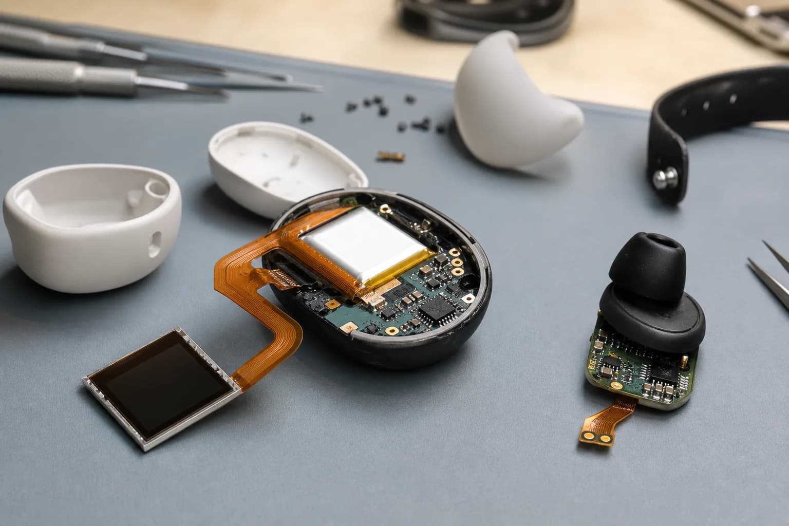
How the board fits the product
A compact consumer product still needs a production-sized review.
Small enclosures, wireless interfaces, battery limits and cost targets all influence stackup, component sourcing, test access and assembly yield.
- Fine-pitch and HDI fanout
- RF, battery and enclosure constraints
- Prototype learning carried into production
Compact HDI01005 PlacementFPC & Rigid-FlexPrototype to Production
Inspection, testing and records
Consumer Product Quality, Test & Production Handoff
Inspection and test follow the device: SPI/AOI and X-ray for assembly quality, electrical coverage, programming, wireless or battery functional checks and the records needed for a repeatable ramp. Quality-system and material-compliance information is confirmed by project scope.
ISO 9001:2015ISO 14001:2015
Build files
Keep the board revision, BOM and assembly drawings together so the factory builds the intended configuration.
Inspection and test
Choose optical, X-ray, electrical or functional checks for the defects that matter to this product.
Material tracking
Agree which material and production records you need to retrieve after shipment.
Design changes
Decide who can approve a material, component or process change before it reaches the line.
Quality documents
Preview & download certificates
The published ISO records name Zhongshan Wenquan Electronic Manufacturing Co., Ltd. and its Zhongshan PCBA facility. They do not certify every PCBArise facility, service or product.
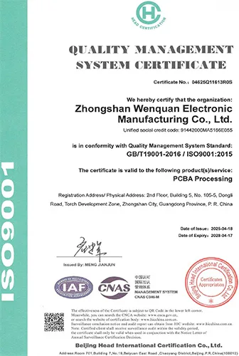
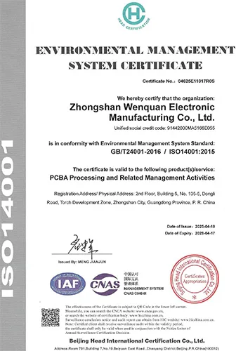
These are management-system certificates, not product or batch COAs. No batch inspection reports or COAs are currently published here.
Frequently asked questions
Common questions about this PCB application
Start with the board, environment and files you have; the detailed route depends on your design.
Can you manufacture wearable and smart-device PCBs?
Yes. We support compact rigid PCB, HDI, FPC, rigid-flex, wireless, battery-management, display, sensor, and fine-pitch assembly projects. The mechanical envelope, antenna area, flexing profile, component package, and production target are reviewed before the build route is confirmed.
Do you support FPC and rigid-flex for wearables?
Yes. FPC and rigid-flex options include PI, PET, and LCP materials, coverlay, stiffeners, ZIF connectors, shielding layers, and surface-mount components. Flex thickness, bend area, bend radius, and dynamic flexing requirements must be confirmed against the released design.
What is the smallest component you can place?
The current assembly reference supports 01005 components, 0.25 mm minimum BGA pitch, and fine-pitch QFP/QFN placement. Exact package, pad geometry, stencil, inspection, and yield requirements are confirmed during DFM/DFA review.
Can you build RF and antenna sections on a consumer device PCB?
Yes. We review stackup, dielectric thickness, ground reference, antenna keepout, matching components, impedance targets, and enclosure interaction. Rogers or other high-frequency materials are considered when the released RF requirements call for them.
How do you move from prototype to production?
The prototype review covers manufacturability, BOM risk, test access, panelization, and the process intended for production. Once the design is released, the same approved data and acceptance requirements can be carried into the production build.
What files are needed for a consumer electronics PCBA quote?
Send Gerber or ODB++ files, BOM, pick-and-place, assembly drawings, 3D or mechanical data where relevant, RF/impedance requirements, test points or fixture requirements, and the target prototype or production quantity.
Related PCB pages
Explore the board and assembly options behind this product.
Use the related PCB, PCBA and quality pages to plan the next part of your build.
PCBArise resource
IoT & Smart Home PCB
Wireless sensors, gateways, smart-home, and connected electronics.
PCBArise resourceFlexible PCB
FPC and rigid-flex for compact and wearable products.
PCBArise resourceHDI PCB
High-density routing and microvia construction.
PCBArise resourcePrototype PCB Assembly
Prototype assembly with a production-aware handoff.
PCBArise resourceComponent Sourcing
BOM review and sourcing support for connected products.
Build the next compact device with a production route in mind.
Share the mechanical envelope, BOM, wireless requirements and target volume for a practical PCB and PCBA review.