
Single flex layer
A simple flexible interconnect between rigid sections where routing density and shielding needs are limited.
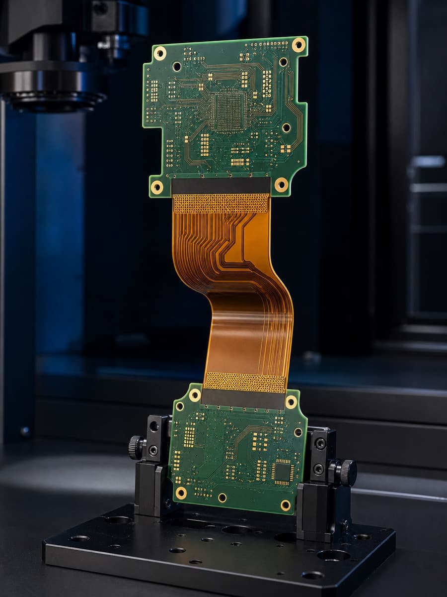
Rigid-flex PCB manufacturing combines fixed component areas and flexible interconnects in one laminated board to reduce connectors and control mechanical transitions.
Rigid-flex success depends on how materials, copper, coverlay and mechanical restraint meet at each transition—not only on the routing inside the rigid areas.
A simple flexible interconnect between rigid sections where routing density and shielding needs are limited.
Two copper layers provide additional routing while keeping the flexible section relatively thin.
Multiple flexible and rigid layers support higher routing density, controlled impedance and compact packaging.
A flex-to-install fold and a repeated-motion hinge require different copper, bend radius and qualification plans.
Layer count alone does not define feasibility. The complete rigid stackup, flexible thickness, bend geometry and transition details are evaluated together.
Electrical and mechanical construction reference
| Total layer count | 2–12 layers |
|---|---|
| Rigid materials | FR-4 and High-Tg FR-4 |
| Flexible materials | Polyimide (PI), adhesiveless copper-clad laminate |
| Flexible area thickness | 0.1–0.6 mm, construction dependent |
| Copper weight | 1/3–2 oz in flexible areas |
| Minimum trace / spacing | 3 / 3 mil standard; 2 / 2 mil advanced |
| Supported features | Coverlay, stiffeners, shielding film, controlled impedance |
| Surface finish | ENIG or ENEPIG; connector finishes by drawing |
| Testing | Electrical test, AOI and application-specific flex testing as specified |
Capability values are design-dependent. Material, copper weight, layer count, via structure, finished thickness and surface finish can change the achievable combination.
The finished outline, bend direction, installed radius and keep-out zones must be defined with the enclosure. Bookbinder allowances may be needed when multiple flex layers bend together.
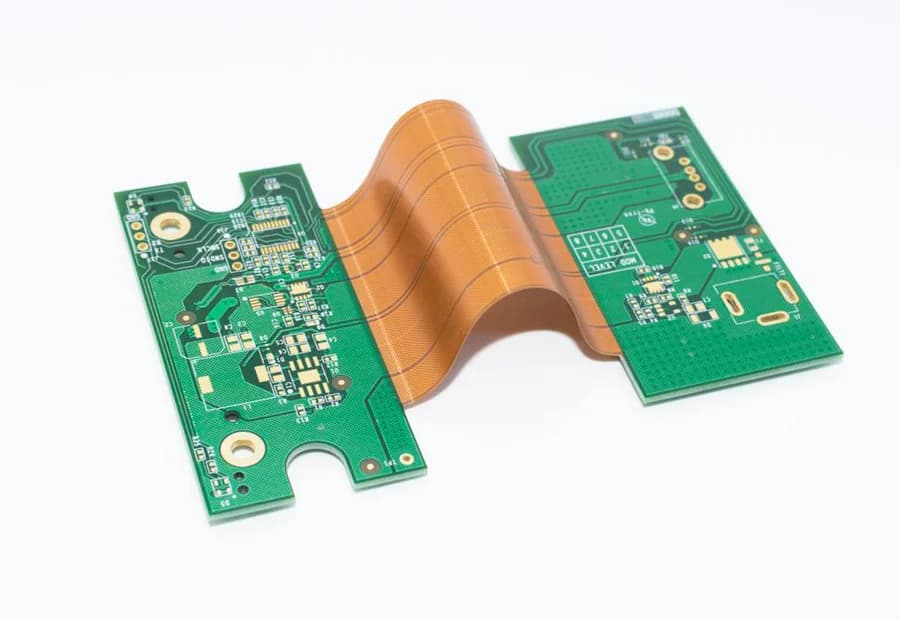
Confirm bend zones, transition geometry, coverlay, stiffeners, via placement and assembly support across the complete rigid-flex outline.
Use these examples as a starting point. The board construction still follows the product’s electrical, mechanical and qualification requirements.
Compact instruments, probes and portable equipment with shaped internal connections.
Weight-sensitive assemblies where connector and harness reduction matters.
Folded optical, display and sensor modules with controlled packaging.
Cameras, sensing assemblies and controls built around constrained enclosures.
Moving or folded internal assemblies that need a defined interconnect path.
Compact, lightweight electronics using both supported component zones and flexible routing.
Quality documents
The published ISO records name Zhongshan Wenquan Electronic Manufacturing Co., Ltd. and its Zhongshan PCBA facility. They do not certify every PCBArise facility, service or product.
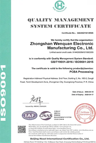

These are management-system certificates, not product or batch COAs. No batch inspection reports or COAs are currently published here.
These answers cover the construction, transition and reliability questions that shape a rigid-flex build.
A flexible PCB remains flexible across most or all of its construction. A rigid-flex PCB permanently laminates flexible layers into rigid board sections, creating one integrated interconnect rather than separate boards joined by connectors.
The published process window supports 2–12 layers. The usable number of flexible layers depends on bend duty, thickness, copper weight and the mechanical design.
Yes. Controlled impedance is available when the material system, dielectric thickness, copper geometry and reference layers are defined across the intended signal path.
Provide the finished outline, rigid and flexible zone boundaries, bend direction, installed bend radius, expected cycle count and any enclosure or assembly keep-out requirements.
Continue to flexible PCB, HDI, DFM review or prototype validation according to the integration risk.
Share the available Gerber, ODB++, drawing, stackup or project requirements with the PCBArise team.