
Quick answer
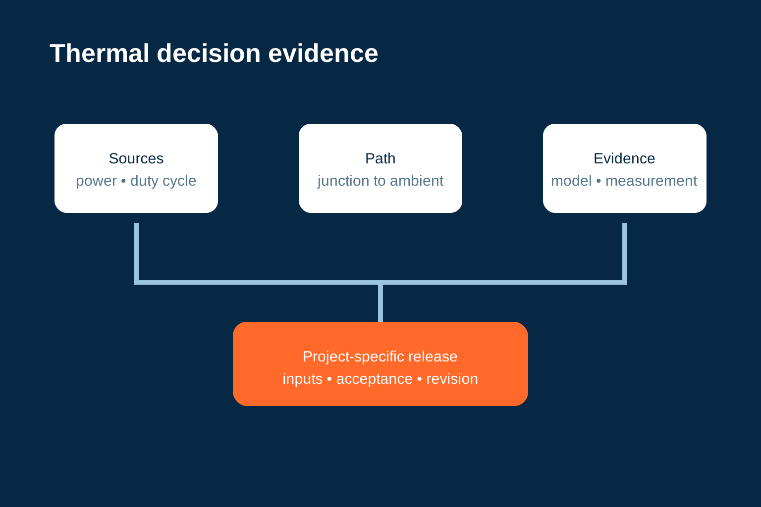
Thermal PCB design begins with a power-loss map, operating states, allowable component and interface temperatures, ambient conditions and the complete path from source to environment. Heavy copper mainly changes current distribution and in-plane or through-layer copper paths; metal-core construction adds a metal spreading structure behind an insulating layer. Compare both against the same model, assembly constraints and project acceptance evidence.
A thermal PCB is a system of heat sources, copper and dielectric paths, interfaces, mechanical contacts and ambient conditions. Choosing heavy copper or a metal-core construction without mapping that system can move heat without solving the limiting interface. A useful supplier review therefore starts with the losses and temperatures the project must manage.
This article owns the cross-route thermal input and decision framework. The Heavy Copper PCB, Metal Core PCB and Power Electronics PCB pages remain commercial capability and application destinations. Any material value, current limit or thermal result must be confirmed for the released project.
Direct answer: when should you choose heavy copper or metal-core PCB?
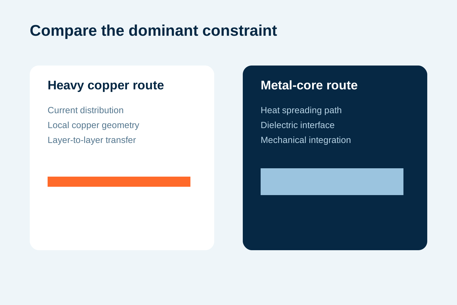
Choose only after mapping electrical current and heat from each component to the final environment. Heavy copper is evaluated when conductor cross-section, current distribution and copper spreading dominate. Metal-core construction is evaluated when heat should cross an insulating layer into a metal spreader or mechanical interface. The correct route depends on dielectric, isolation, geometry, assembly and cooling conditions.
Build a thermal input map before the stackup
List each significant loss source by operating state: continuous, intermittent, startup, overload and fault where relevant. Record how loss was derived, the temperature limit that governs it, ambient range, airflow or enclosure assumptions, mounting orientation, nearby heat sources and the intended external sink or chassis interface.
Component datasheet thermal metrics describe defined test conditions, not the final board automatically. Texas Instruments and Analog Devices both emphasize the PCB path around exposed pads and vias. Treat package guidance as an input to the application model, then check the actual land pattern, solder connection, copper network and boundary conditions.
Separate inputs, paths and evidence
| Decision input | Questions to answer | Evidence to retain |
|---|---|---|
| Heat and current sources | Where, when and how much loss or current occurs? | Calculation basis, operating states and revision |
| Temperature limits | Which component, dielectric, solder joint or interface governs? | Datasheet or project requirement and margin basis |
| Boundary conditions | What ambient, airflow, enclosure and mounting apply? | Model inputs and test setup description |
| Board construction | Which copper, dielectric, vias or core carry heat and current? | Released stackup and geometry |
| Acceptance | What will be modeled, measured or inspected? | Method, locations, states, limits and owner |
Heavy copper changes more than conductor area
Heavier copper may support a current-distribution or heat-spreading objective, but the finished result also depends on trace neck-downs, pads, plated holes, layer transitions, copper balance, etching and the dielectric stack. The critical bottleneck may sit at a connector, terminal, via field or component land rather than in the widest copper region.
Give the fabricator a current map and the geometry that cannot change. Ask how finished copper affects line and spacing, plated features, registration, stackup symmetry and the chosen surface finish. Avoid converting a generic current chart into a project rating without the same conductor geometry, temperature-rise basis and environment.
Metal-core construction adds an interface-driven route
An insulated metal substrate or other metal-core construction places a metal layer behind a dielectric system so heat can spread toward a mechanical interface. The dielectric remains part of the thermal and electrical path. Its thickness, electrical requirement, material system, copper pattern, core geometry and contact to the external structure must be reviewed together.
The metal core does not by itself define junction temperature. Solder coverage, component pad, dielectric, board-to-sink contact, interface material, flatness, fasteners, airflow and the sink or chassis can dominate different portions of the path. State whether the board is the final heat spreader or one link in a larger cooling assembly.
Heavy copper versus metal core
| Question | Heavy-copper route | Metal-core route |
|---|---|---|
| Primary design focus | Current distribution and copper conduction within a multilayer or rigid construction | Heat transfer through dielectric into a metal spreading or mounting structure |
| Critical inputs | Current map, duty cycle, copper geometry, layer transfer and allowable rise | Loss map, dielectric system, isolation need, core and external contact conditions |
| Assembly interaction | Thermal mass, pad design, soldering and terminal attachment | Pad design, soldering, board support, flatness and mounting interface |
| Evidence question | Do the released conductors and transitions meet electrical and thermal acceptance? | Does the complete source-to-environment path meet the project temperature requirement? |
Some designs can combine approaches; others are constrained by routing density, double-sided assembly, isolation, mechanics or cost. The comparison should be performed on the same operating cases and acceptance method, not on unrelated headline properties.
Thermal vias and copper planes need a defined destination
Vias can connect a component land to internal or opposite-side copper, but their effect depends on placement, finished hole, plating or fill, solder process and the area available to receive and reject heat. Analog Devices cautions that exposed-pad electrical potential must also be checked from the component documentation. A thermal via is not useful merely because it appears under a package; the downstream path and assembly method must be intentional.
Ask the component supplier, PCB fabricator and assembler to review the same land pattern. Via-in-pad treatment, solder wicking risk, stencil design, void acceptance and inspection may affect the thermal connection. These choices belong in the fabrication and assembly package.
Model and measurement must share conditions
Document material properties and interface assumptions used in simulation, including their source and temperature basis. Define power states, ambient, airflow, mounting, emissivity assumptions if relevant and where temperature is evaluated. For measurement, state sensors or imaging method, locations, stabilization criteria, operating load and uncertainty.
A model can compare candidate paths; a prototype measurement can test the assembled system under stated conditions. Neither becomes a universal board rating. Keep the evidence with the exact board, component, assembly and mechanical revisions it represents.
Thermal route review flow
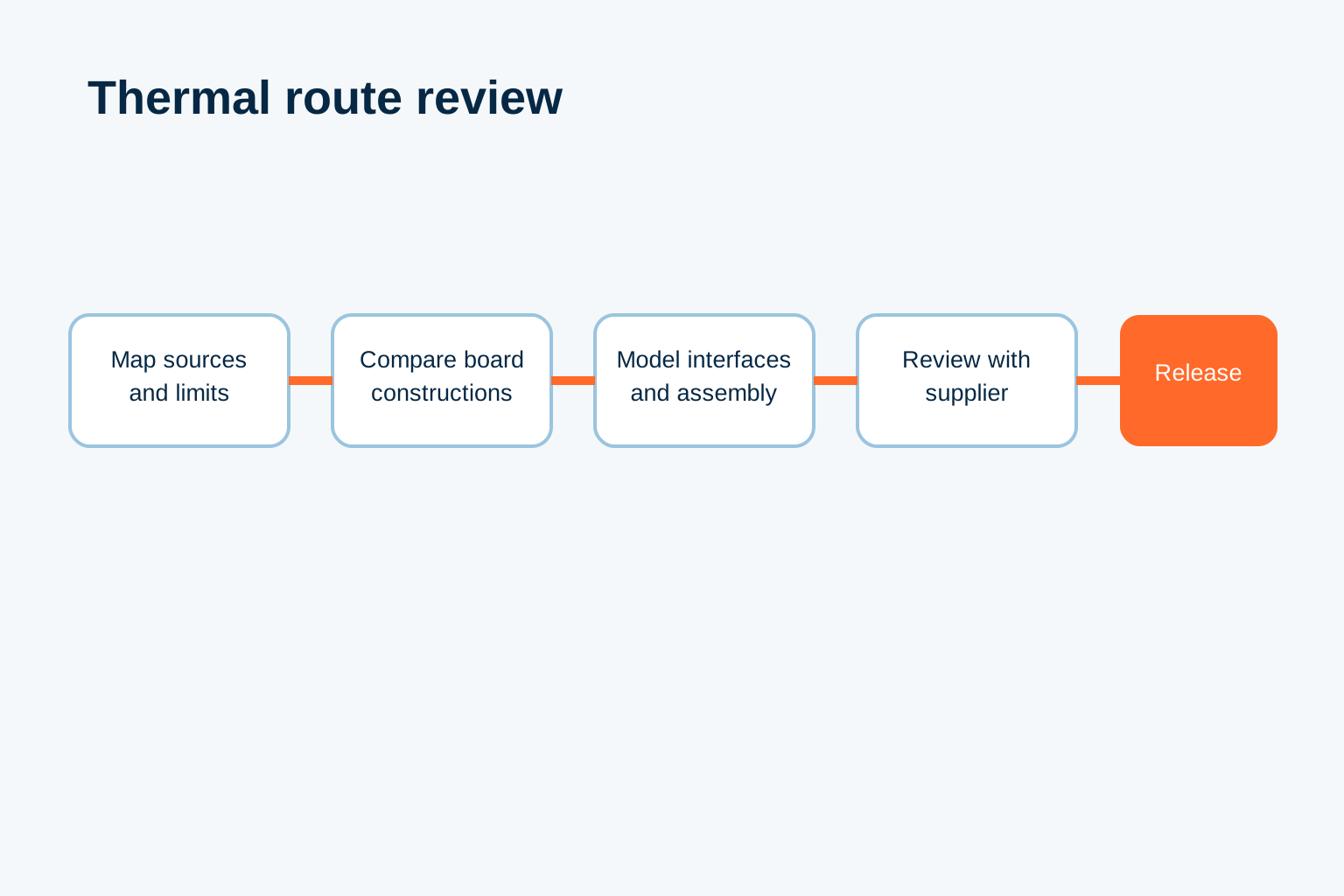
- Map loss sources, current paths, operating states and governing temperature limits.
- Define ambient, airflow, enclosure, mounting and external sink interfaces.
- Compare conventional, heavy-copper and metal-core constructions against those inputs.
- Model copper, dielectric, vias, packages, contacts and external cooling as one path.
- Review fabrication, assembly, inspection and mechanical constraints with suppliers.
- Release the selected stackup, acceptance method and revision-controlled evidence plan.
Thermal PCB quotation checklist
- Gerber or ODB++, drill, stackup and controlled mechanical drawing.
- Component list, placement and identified heat or current sources.
- Operating states, duty cycle, ambient and cooling conditions.
- Allowable temperatures or rises and the source of each limit.
- Copper, dielectric, core, via and isolation requirements.
- Exposed-pad, stencil, solder, inspection and assembly requirements.
- External sink, chassis, interface material, fastener and flatness constraints.
- Model, prototype test, reporting and change-approval expectations.
Submit the controlled package through Get a Quote for a project-specific PCB manufacturing review. Include unresolved assumptions so engineering feedback can close them before the thermal route is released.
Engineering review
Prepared and reviewed for project use
Engineering Director
Senior Quality Engineer
Review scope: technical accuracy, evidence wording, standards references, internal links and release readiness. Project requirements remain subject to the released files, applicable acceptance criteria and agreed test documentation.
FAQ
Questions engineers ask before release
Is heavy copper PCB better than metal-core PCB for heat management?+
Neither is universally better. Heavy copper is often evaluated for current distribution and copper conduction; metal-core construction is evaluated for transfer through an insulating layer into a metal spreader. Compare both against the same sources, interfaces and acceptance conditions.
What inputs are needed for thermal PCB design?+
Provide component losses and current paths, operating states, temperature limits, ambient and airflow, enclosure and mounting, stackup, copper and via geometry, external heat-sink interfaces, assembly details and the intended model or test method.
Do thermal vias always reduce component temperature?+
Their effect depends on the land pattern, via construction, solder process, connected copper and where that copper rejects heat. Review the complete path and the component manufacturer's electrical and assembly guidance.
Can a component datasheet thermal value predict the final PCB temperature?+
Not by itself. Datasheet metrics use defined test conditions. The final result also depends on the board, solder connection, nearby components, mounting, airflow, enclosure and external cooling interfaces.
How should a thermal PCB design be validated?+
Use a documented model and/or prototype measurement with stated power, ambient, airflow, mounting, sensor locations and acceptance limits. Keep results tied to the exact board, component, assembly and mechanical revisions.
What should I send for a heavy-copper or metal-core PCB quote?+
Send fabrication data, stackup, placement, current and loss maps, operating conditions, temperature limits, material and isolation needs, thermal interfaces, assembly requirements and the requested inspection or evidence plan.
Reference points
Sources and verification starting points
External standards and industry references help frame the decision. Confirm current supplier evidence and project-specific requirements before release.
- Texas Instruments — PCB thermal design technical article
- Texas Instruments — thermal design application report
- Texas Instruments — exposed-pad and thermal-via application report
- Analog Devices — exposed-pad design note
- Analog Devices — thermal considerations for exposed-paddle packages
- Sierra Circuits — professional stackup trade-off discussion