
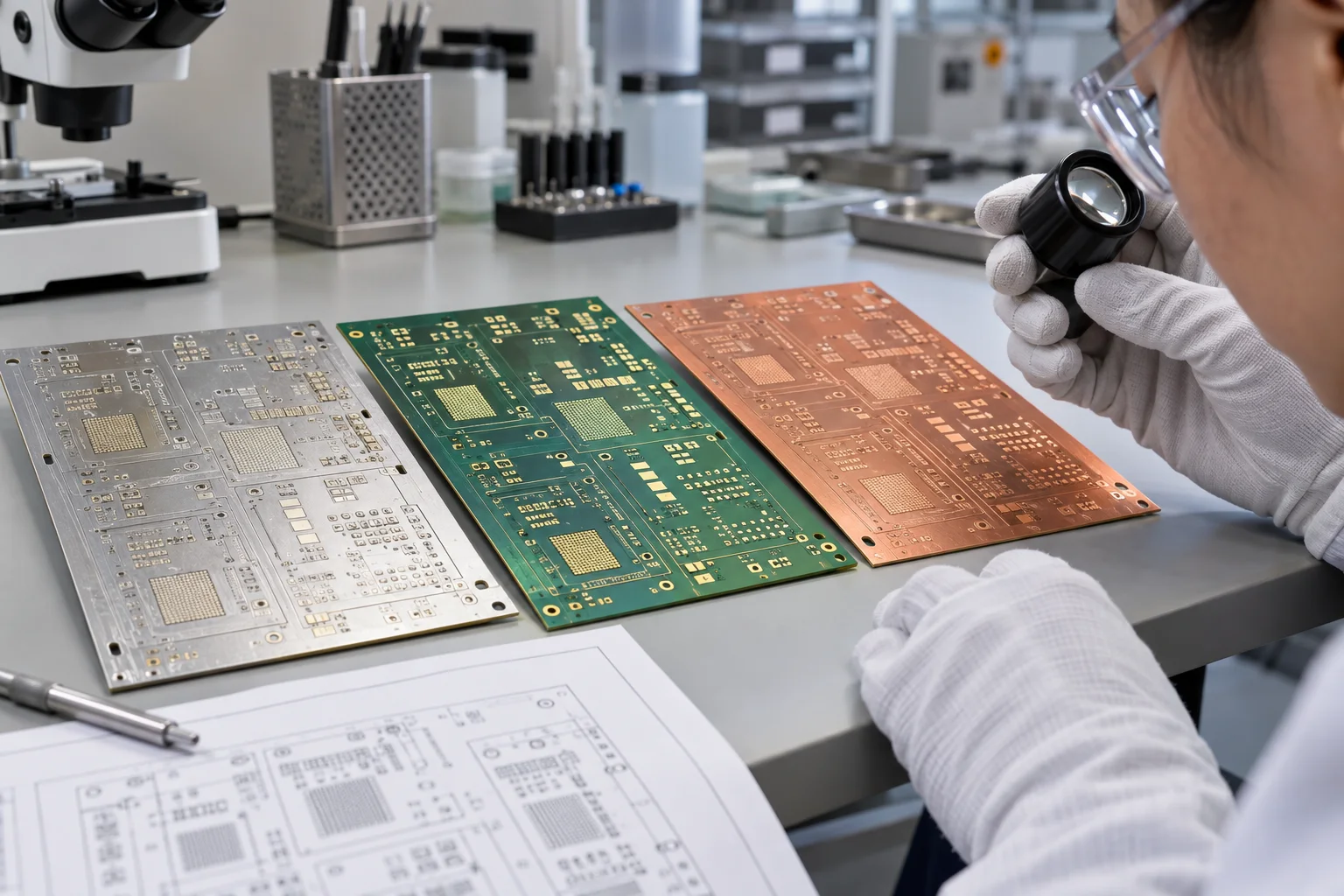
In short
Choose the finish for the most demanding pad on the board. Lead-free HASL is a practical general-purpose finish where solder-planarity risk is low; ENIG gives a flat nickel/gold surface for dense SMT and longer storage planning; OSP keeps pads flat at lower finish cost when the board can move through a defined assembly window. Put the finish on the fabrication drawing, then check it against package pitch, reflow count, test contacts and storage handling.
- Use lead-free HASL for a robust, general-purpose solderable finish when pad flatness is not the limiting constraint.
- Use ENIG when the board needs a flat surface for dense SMT or a longer, controlled storage plan; it is not a blanket reliability upgrade.
- Use OSP when a fast, controlled SMT route and finish cost matter; plan handling and repeated thermal exposure around the chosen OSP process.
- Name the finish, assembly sequence, storage expectation and any special contact areas in the fabrication package.
ENIG, lead-free HASL and OSP protect exposed copper until assembly, but they solve different manufacturing problems. Pick the finish from the board’s tightest package, the number of heat cycles, how long the bare boards may wait, and whether exposed pads also serve as test or contact surfaces. For a buyer comparing quotes, the useful question is not “which finish is premium?” It is “which finish keeps this released design solderable without adding a cost or handling risk we do not need?”
Which finish should you choose first?
Start with the most demanding assembly feature. A through-hole-heavy control board with generous pad spacing may accept lead-free HASL well. A dense QFN, BGA or fine-pitch connector shifts the decision toward a flat finish—often ENIG, sometimes OSP when the assembly route and handling are deliberately controlled. If the board will sit in stock, travel through multiple internal handoffs, or be assembled in more than one operation, make that storage and thermal sequence explicit before selecting OSP.
| Finish | What it gives the buyer | Where it needs care | Good first fit |
|---|---|---|---|
| Lead-free HASL | A solder-coated, general-purpose finish with familiar solderability. | The leveled solder surface is less planar than immersion finishes; assess dense or very small SMT lands rather than assuming they will print the same way. | Boards with generous pad geometry, through-hole content or uncomplicated SMT. |
| ENIG | A flat nickel/gold finish that suits dense SMT land patterns and a longer planned bare-board storage interval. | It adds process and material cost. Define requirements and incoming checks instead of treating the gold appearance as proof of a good solderable surface. | Fine-pitch SMT, BGA/QFN-heavy layouts, or programmes that need a controlled storage plan. |
| OSP | A very flat organic protection over copper, commonly considered where finish cost and high-volume SMT flow matter. | Its protective film is handling- and thermal-history-sensitive. Align storage, reflow and test contact use with the assembler’s approved OSP process. | Fast, controlled SMT flow where the assembly route is known before boards are released. |
This is a decision table, not a PCBArise capability claim or a substitute for a component supplier’s land-pattern guidance. The Ansys assembly design review and IPC’s BGA implementation guide both treat finish as one input among land pattern, paste, stencil, thermal profile and inspection—not as a stand-alone yield guarantee.
How do flatness and soldering change the choice?
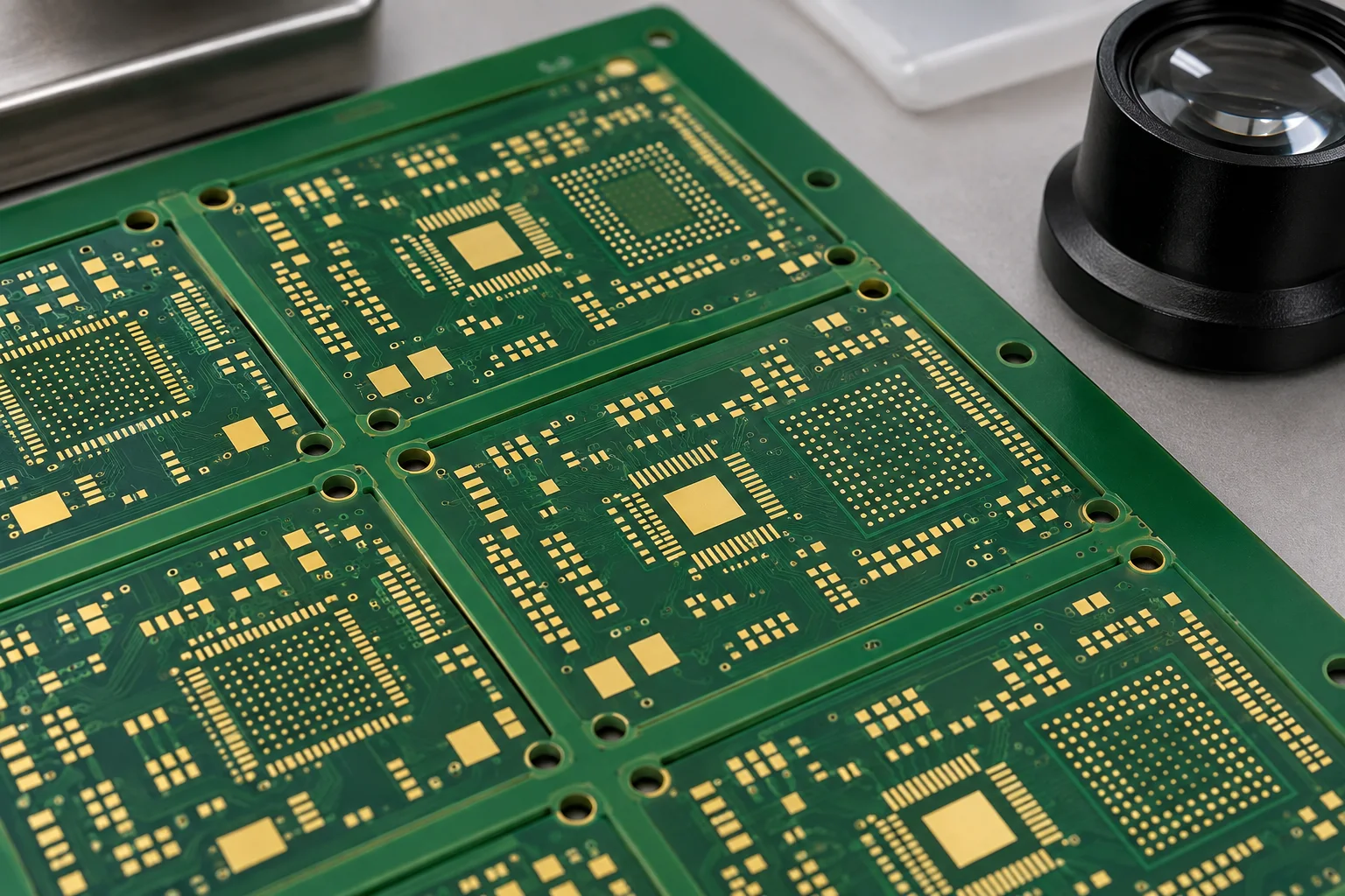
HASL leaves solder on exposed copper and is leveled with hot air. Its surface is not as coplanar as ENIG or OSP, so a close-pitch land pattern has less margin for uneven paste contact and component seating. That does not make HASL wrong for every SMT board; it means the smallest package, not the average resistor, should set the rule. Put the package pitch, land pattern source and assembly side count in the release so the finish is evaluated against the actual board.
ENIG deposits nickel under a thin immersion-gold layer. The visible gold is a protection layer, not a reason to request “more gold.” Its flatness is useful where paste printing and placement need consistent pad geometry. Ask the fabricator to identify the applicable finish specification and the assembler to confirm that the component finishes, paste and reflow route are compatible. A finish selection cannot repair an unsuitable footprint or stencil aperture.
OSP is an organic protective film over copper. It gives a flat land, but it is intended to be managed as part of the assembly process rather than handled like a durable connector coating. If fixture probes, repeated rework or a long queue before assembly are likely, call those out early. The Global Electronics Association’s OSP task group exists precisely because OSP evaluation includes chemistry, solderability and process handling—not just a price comparison.

What should you write on the fabrication drawing?
Write the finish by name, not as “gold finish” or “lead-free finish.” Then add the decisions that change whether it can be assembled:
- Surface finish: “ENIG,” “lead-free HASL,” or the approved OSP process named in your purchasing specification.
- Assembly route: board sides, expected reflow or selective-solder sequence, and whether the build includes later hand soldering or rework.
- Storage and handling: the expected gap between fabrication and first assembly, plus any controlled packaging or bake restrictions supplied by the chosen finish process.
- Special surfaces: test points, press-fit zones, wire-bond areas and edge contacts. These may require a separate surface treatment; do not silently assume one finish serves every function.
- Acceptance basis: the customer specification or applicable standard revision and any required supplier documentation.
Surface finish: [ENIG / lead-free HASL / approved OSP]. Assembly: [one/two] SMT side(s), [reflow/selective/hand] operations as listed in the build notes. Bare boards are to be packed and handled for the stated finish process until first assembly. Identify any test contacts, edge contacts or special pad areas that require a different treatment before tooling.
That note makes the quote comparable: one supplier is not pricing an unspecified “gold board” while another prices a standard ENIG process. It also gives P2 procurement teams a concrete way to compare exclusions without confusing a service-page option list with a project promise.
How do storage, testing and cost alter the answer?
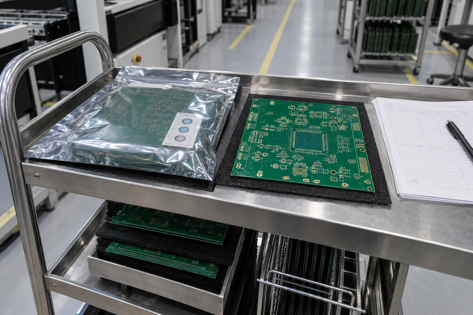
Storage is part of the finish decision because bare boards are not all consumed on the day they leave fabrication. ENIG is often selected where a longer planned storage interval is useful, while OSP needs a more deliberate route from fabrication to assembly. Do not copy a generic shelf-life number into your drawing: the applicable value depends on the finish process, packaging and customer specification. Instead, state your expected timing and ask the supplier to document the process basis used for that build.
For test contacts, consider whether probes will repeatedly touch exposed finish without soldering. For edge connectors or wear surfaces, hard gold or another dedicated treatment may be needed; none of ENIG, HASL or OSP should be assumed to replace a specified contact finish. Cost also needs context. ENIG’s chemical process and precious-metal content can make it a higher line item, but the relevant comparison is the cost of the finish against the risk of a pad surface that does not suit the smallest package or planned build flow.
Three finish-selection mistakes to avoid
- Choosing by colour: “gold” does not identify ENIG thickness, process control or a special connector coating. Name the actual finish and acceptance basis.
- Letting the easy component decide: a board can have hundreds of forgiving passives and one fine-pitch device that drives the pad-flatness requirement.
- Forgetting the post-fab journey: the finish decision must survive storage, transport, assembly sides, test and rework—not only the initial quote.
For a production-ready comparison, send the fabrication drawing, Gerber or ODB++ package, BOM, component land-pattern constraints, assembly sequence and expected storage plan together. The PCB manufacturing page explains the service context; those project files define the finish decision for a real build.
About the author
PCBArise Electronics
PCBArise Electronics publishes this guide to help design and NPI teams prepare clearer manufacturing files. The requirements for any actual build are confirmed from its current design package.
FAQ
Common questions
Is ENIG always better than HASL or OSP?+
No. ENIG is a strong choice when flat pads and planned storage matter, but it costs more and does not replace good land patterns, paste design or process control. Lead-free HASL can fit boards with forgiving geometry, while OSP can fit a controlled, fast SMT route. Choose from the limiting package and build sequence.
Is lead-free HASL suitable for fine-pitch PCB assembly?+
It can be suitable only if the actual land pattern and assembler process have enough planarity margin. Treat the smallest-pitch part as the decision point, review its footprint and stencil, and do not infer suitability from the board’s larger components.
When should I choose OSP?+
Choose OSP when you need a flat surface and can control the route from fabrication through assembly, including storage, handling and thermal exposure. Put that route in the manufacturing brief; OSP is not a universal substitute for a durable test-contact or connector finish.
What PCB surface finish should I specify for BGA or QFN pads?+
Start with a flat finish such as ENIG or an approved OSP route, then verify the exact land pattern, solder paste, stencil and reflow plan for the package. The finish alone does not prove a BGA or QFN will assemble correctly.
Do ENIG, HASL or OSP work for edge contacts?+
Do not assume so. Edge contacts and wear surfaces can require a dedicated hard-gold or selective-contact treatment. Identify those areas separately on the drawing so the fabricator does not apply the ordinary solderable finish to a wear function.
Technical references
Sources used for this guide
These sources explain the standards, materials or process details discussed above. Check the current revision when applying them to a new design.