
In short
Give the fabricator an impedance table, not a single “controlled impedance” note. For each net class, state the routing layer, single-ended or differential target, tolerance, reference plane, expected trace geometry and whether the fabricator may adjust it. Attach the proposed stackup, material and copper requirements, then agree on the coupon and test report before fabrication.
- List every impedance-controlled net class with its layer, target, tolerance and reference plane.
- Show the proposed stackup and identify which dimensions or materials are fixed versus adjustable.
- Separate design trace geometry from finished-board geometry; agree on any fabricator adjustment before it changes routing intent.
- Specify whether test coupons and a measured impedance report belong in the delivered build package.
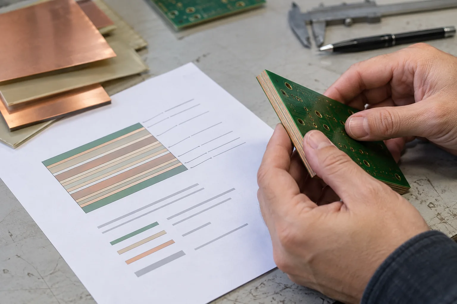
Before routing, write down which traces need which impedance on which layers. A board-wide note such as “100 Ω differential impedance” leaves the fabricator guessing about the pair, its reference plane and acceptable variation. A useful handoff contains an impedance table plus a proposed stackup. It identifies what the designer has already fixed and what the fabricator can adjust to hit the electrical target.
What belongs in the impedance table?
Make one row for each controlled net class. Name the nets or class, identify single-ended or differential impedance, routing layer, reference plane, target, allowed tolerance, nominal width and differential spacing where applicable. Say whether those dimensions are design constraints or starting values the fabricator may adjust. Westak’s stackup checklist and Altium’s fabrication-drawing guide both show why an impedance number without layer and geometry is incomplete.
| Field to write | Example entry (illustrative) | Why the shop needs it |
|---|---|---|
| Net class / layer | USB_RX/TX pair on L3 | Connects a test target to the routed geometry. |
| Target / tolerance | 90 Ω differential, ±10% at coupon | States the measurable requirement; values here are an example, not a PCBArise capability claim or a USB design rule. |
| Reference | Solid L2 ground plane | Defines the return path assumed by the field solver. |
| Geometry | CAD width and gap per attached stackup drawing; fabricator to propose final etched dimensions | Distinguishes drawn features from what is manufactured. |
| Verification | Same-panel coupon matching L3 structure; report measured differential impedance | Defines what will actually be measured and delivered. |
The sample is a form-fill example. Replace its target, tolerance, layer and net class with requirements from the interface specification and signal-integrity design. It is not a universal 90 Ω rule; neither is ±10% a promise that PCBArise can make for every construction.

A fabrication note you can adapt
Put the table above on the fabrication drawing or in an attached impedance schedule. Then add a note like this, replacing every bracketed item with your design data:
Controlled nets: [net class] on [signal layer], referenced to [plane layer], [single-ended/differential] target [Ω] with [tolerance] at the specified coupon. Nominal CAD trace width [value] and pair gap [value]. Fabricator may propose changes to [allowed width/gap or dielectric thickness] before tooling; do not change [fixed board thickness, material family, plane assignment or pair spacing] without designer approval. Use a same-panel coupon representative of the finished structure and include the measured result with the shipment.
If the fabricator owns width compensation, include enough routing clearance for that adjustment. If the designer owns a hard width or gap—for example, because the BGA escape cannot grow—mark it fixed. Do not approve a stackup that reaches the target by altering a non-negotiable mechanical or routing constraint.
Which stackup details change the impedance result?
Provide the layer order, intended signal and plane assignments, core and prepreg construction or acceptable material family, finished board thickness, finished copper requirements, solder-mask treatment over controlled traces and any specified dielectric-property basis. Trace width, pair gap, dielectric thickness, copper geometry and the reference plane all affect impedance. Polar Instruments’ stackup guidance explains why calculated values need the actual manufacturing construction, rather than only a CAD default.
For a high-frequency design, give the frequency or rise-time context used to choose a material, and state if a particular laminate is mandatory. Do not substitute a generic “FR-4” name for a material requirement when loss or dielectric behavior is part of the design. The related RF stackup guide covers material selection in more detail; this page is about the handoff document.

Who may change trace width or dielectric thickness?
Choose one owner for each variable in the drawing. A common route is for the designer to set the electrical target, layer assignment, plane and maximum geometry envelope, while the fabricator proposes exact dielectric thickness and finished trace width after selecting its available materials and process compensation. A second route is a fully locked stackup and geometry; that gives the fabricator fewer knobs and can require a different material or process. Neither route works if the handoff silently mixes a locked CAD width with a note allowing unrestricted width adjustment.
When the fabricator proposes a different dielectric thickness, revisit both impedance and the overall thickness, via aspect ratio, coupling to adjacent layers and any connector or enclosure fit. The change is not just a number in a solver.
How should impedance be checked on the finished build?
State the coupon construction, target, tolerance, measurement method and reporting expectation. A coupon should represent the relevant routing layer and reference plane and travel through the same panel process as the boards. Polar’s controlled-impedance booklet discusses time-domain-reflectometry measurement and the relationship between coupon and board. A passing coupon indicates the sampled structure met its specified measurement; it does not prove that every routed trace has the intended geometry, or that the complete channel meets a system eye-diagram limit.

Three mistakes that waste a stackup review
- One target for the whole board: different layers and structures can have different geometry. Tie each target to its layer and net class.
- Width and gap with no ownership: a proposed process adjustment may no longer fit the BGA escape. Mark fixed limits and keep clearance for any allowed change.
- A test request with no coupon definition: a report cannot answer the buyer's question if it measures the wrong layer or structure. Match coupon construction to the routed signal.
For a manufacturing discussion, send the drawing, impedance table, proposed stackup, Gerber or ODB++ files and any channel constraints that cannot change. The PCBArise materials and stackup page describes the service context; the actual design package supplies the electrical requirement.
About the author
PCBArise Electronics
PCBArise Electronics publishes this guide to help design and NPI teams prepare clearer manufacturing files. The requirements for any actual build are confirmed from its current design package.
FAQ
Common questions
What should I put on a controlled-impedance PCB fabrication drawing?+
Add an impedance table with net class, layer, reference plane, single-ended or differential target, tolerance, nominal width and pair gap where relevant. Attach the proposed stackup and state which dimensions the fabricator may adjust.
Is “100 Ω differential” enough to specify an impedance stackup?+
No. Identify the affected pair and routing layer, reference plane, acceptable tolerance, geometry and coupon/test expectation. The same target can require different widths on different layers.
Can the PCB fabricator change my trace width?+
Only within the adjustment envelope you explicitly allow. State fixed width or gap limits near escapes and review a proposed finished geometry before tooling; if there is no room for a change, lock the dimension and solve the stackup around it.
Does an impedance coupon prove every trace on the PCB is correct?+
No. It checks a representative structure manufactured with the panel. Use the same relevant layer and reference-plane construction, request the measured result, and keep channel-level performance testing separate.
Do I need to name the exact laminate in the stackup?+
Name it when material properties or qualification require that specific laminate. Otherwise give an acceptable material family and dielectric-property requirement, and show which substitutions need design approval before fabrication.
Technical references
Sources used for this guide
These sources explain the standards, materials or process details discussed above. Check the current revision when applying them to a new design.