
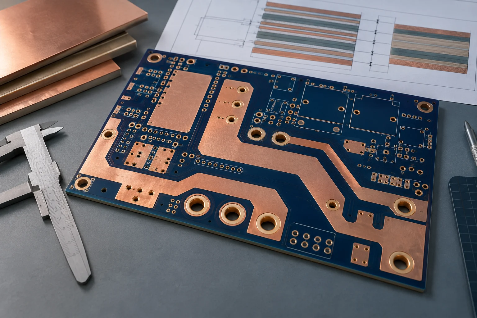
In short
For a power PCB, name each current path and operating case first. Then state the permitted temperature rise, minimum finished copper on each affected layer, trace or plane geometry, and every bottleneck such as a neck-down, via field or terminal pad. Outer-layer plated copper changes the finished thickness. Release the current map, stackup and drawing note together so the construction is unambiguous.
- Size each conductor from its current, duty cycle, allowed rise and complete geometry; one “amps per ounce” rule cannot describe a power board.
- State base foil and minimum finished copper separately where outer-layer plating matters, especially at traces, pads and plated holes.
- Check bottlenecks, vias, connector pads and layer transitions—not only the widest copper pour—before calling a current path adequate.
- Put the current map, stackup, copper callouts and test or temperature acceptance method in the same release package.
Specify copper weight for the whole current path, not by asking how many amps one ounce of copper can carry. Start with the current in each operating state, the temperature rise your product can tolerate, and the narrowest feature in the path. Then tell the fabricator which layers carry that current, the base foil, the required finished copper, trace or plane geometry, plated-hole requirements and the stackup. That gives a power, industrial-control or high-current NPI team a buildable instruction instead of a guess disguised as a copper callout.
What copper weight should a power PCB specify?
Choose the finished conductor cross-section that meets the stated current and temperature limit at the path’s narrowest point. A wide outer-layer pour, a short inner-layer neck-down and a small plated-hole barrel do not carry heat or current in the same way. IPC-2152 frames conductor sizing around current-carrying capacity and acceptable temperature rise; it is a much better starting point than a universal “ampacity per ounce” chart because the board construction and environment matter.
First separate the electrical job from the purchasing shorthand. “One-ounce copper” commonly names the starting foil weight, while an outer layer can gain copper during through-hole plating. For a board whose current flows through outer traces, pads and vias, the drawing needs the minimum finished copper where it matters. For an internal plane, name the foil or finished copper specified by the approved stackup. Do not leave the fabricator to infer whether a copper number is a base foil, a nominal stackup entry or a guaranteed finished feature.
| Power-path condition | What to define | Why it changes the copper decision |
|---|---|---|
| Continuous load | Normal current, ambient, allowed temperature rise and run time. | Sets the steady-state heating case for traces and planes. |
| Pulse, startup or fault | Peak current, duration, repetition and protective-device behaviour. | A short pulse may be acceptable electrically yet still expose a via, terminal or neck-down as the limiting feature. |
| Outer conductor | Base foil, plating contribution, minimum finished copper, width and exposed or covered condition. | Outer copper exchanges heat with the environment and is changed by plating; finished thickness is the useful fabrication instruction. |
| Inner conductor | Layer, copper thickness, trace or plane geometry, neighbouring planes and dielectric context. | It sheds heat through the stackup, so it cannot be sized as if it were an isolated external trace. |
| Transition or termination | Via count, hole and pad geometry, connector pad, soldered lug or busbar interface. | The path fails at its smallest cross-section, not at its largest pour. |
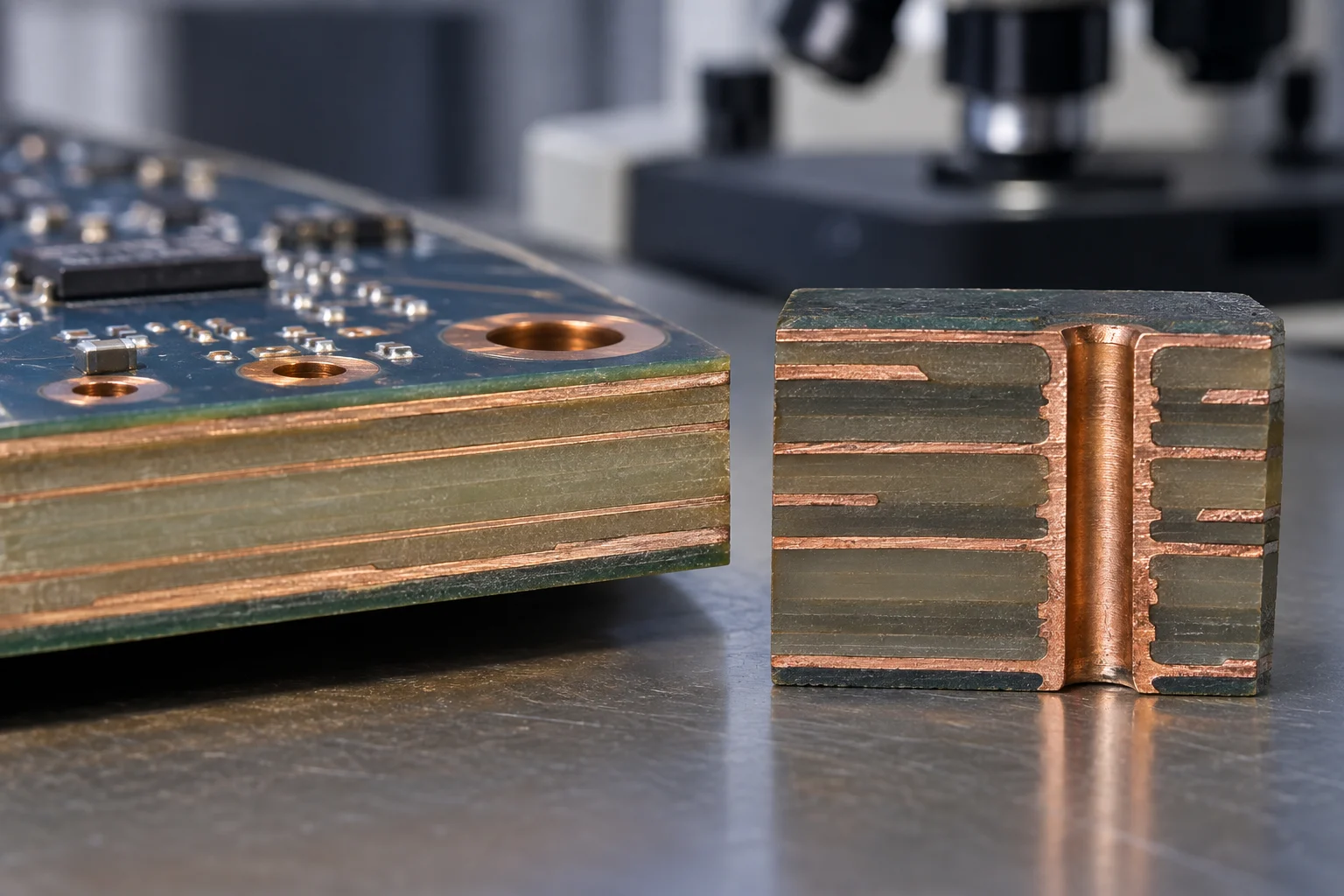
How do current and temperature rise set the first copper choice?
Make a current map before choosing copper. Mark every source, load, branch, return path, fuse, terminal and layer transition. For each segment, record continuous current, peak current, duty cycle, ambient condition and the temperature rise it may add without violating a component, connector, insulation or enclosure limit. That map is what a trace-width calculation, simulation or prototype measurement must represent.
Then calculate or model the conductor using the actual board conditions: its width and finished thickness, whether it is external or internal, distance to planes, board thickness, copper area, airflow and the allowed rise. IPC’s technical discussion of IPC-2152 notes that copper cross-section alone does not tell the whole story; nearby planes and the environment alter the result. Treat a calculator result as a first design value, not as permission to ignore a connector pin, neck-down, via barrel or a hot enclosure.
For a dense power layout, distribute current across parallel copper only when the geometry really shares it. Two nominally parallel paths can divide unequally if one has a longer route, a thinner section, more vias or a higher-resistance joint. Include the return path too: a supply plane may look generous while its return is forced through a narrow bridge. A power path is a loop, not a single highlighted polygon.
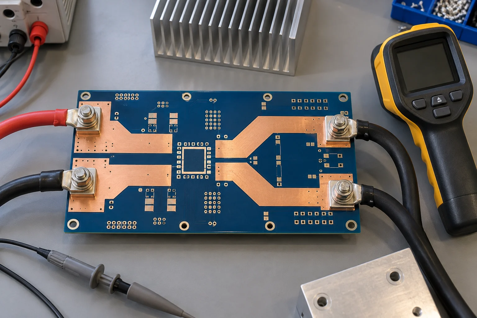
Why do base foil and finished copper need separate callouts?
Because fabrication changes an outer-layer conductor. Starting foil is laminated into the board; later plating builds copper in holes and on exposed outer-layer features. If the product needs a minimum cross-section after fabrication, calling out only a foil weight can leave the drawing ambiguous. Conversely, asking for an unusually heavy finished outer layer without showing the trace spacing, drills, pads and stackup hides the manufacturability trade-off.
Write copper information at the level that controls the decision. A stackup table should show each layer’s intended copper construction. A fabrication note should identify any minimum finished outer copper or plated-hole requirement that is critical to the power path. The gerber or intelligent manufacturing data should preserve the actual neck-downs, clearances and copper balance. If a supplier proposes a material or plating change, compare it against the declared finished thickness and current map before accepting it.
Power-path requirement: identify the released current map in drawing [reference]. Layers [L1 / L2 / ...] carry the named power and return paths. For each marked outer-layer conductor, minimum finished copper is [value and unit]; base foil is [value and unit] where specified by the stackup. Preserve the released trace, plane, via and terminal geometry. Report any change that reduces a marked conductor cross-section, alters the stated stackup, or changes the plated-hole construction.
The brackets are deliberately inputs, not invented values. Fill them from the electrical calculation, stackup and component or terminal requirements. This is more useful than a blanket “heavy copper required” note because it tells a fabricator which path is critical and gives procurement a like-for-like basis for comparing a standard construction with a heavier one.
When does heavier copper help—and when does it create another constraint?
Heavier copper helps when conductor cross-section, voltage drop or copper spreading is the limiting part of a defined path. It can reduce resistance in a given geometry and can change how heat spreads within the board. It does not automatically solve heat transfer from a component into the enclosure, nor does it repair a small terminal, insufficient via array, unsuitable dielectric, or a hot ambient condition. The related thermal PCB guide separates copper conduction from the complete route to the environment.
More copper also affects etching, line and space, copper balance, plated-hole aspect choices, stackup thickness, drilling and assembly thermal mass. A pad connected to a large plane may need a released thermal-relief or soldering strategy; a fine feature that was comfortable at lighter copper may need more space. This is not an argument against heavier constructions. It is the reason to specify the current-bearing layers and geometries early, rather than upgrading copper after the rest of the layout has frozen.
What should a fabricator and assembler receive?
Send the electrical intent and the physical construction together. At minimum, include Gerber or ODB++ data, a stackup, the fabrication drawing, net or region identifiers for critical current paths, component placement and the operating cases that drove the copper decision. Add the terminal, press-fit, busbar, soldering or connector constraints that can turn a board-level copper decision into an assembly problem.
- Current map: named supply and return paths; continuous, peak and duty-cycle cases; the intended branch sharing.
- Temperature basis: ambient, airflow or enclosure assumptions and the allowed rise or relevant temperature limit.
- Stackup: layer order, copper construction, dielectric family and any required finished-thickness control.
- Geometry: locked widths, clearances, plane bridges, via arrays, terminal pads and copper keep-outs that cannot be reduced.
- Assembly interaction: components with heat-sensitive or high-mass joints, soldering method, external copper or busbar interfaces and required board support.
- Acceptance method: calculation, thermal model, prototype measurement or another defined evaluation tied to the actual revision and operating state.
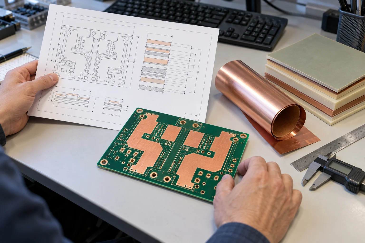
Four power-board copper mistakes to avoid
- Using one current number for the whole board: branches, startup events and returns can have different limits. Size each path and its bottlenecks.
- Calling out only “2 oz”: say where it applies and whether the critical requirement is base foil or minimum finished copper.
- Checking only trace width: inspect vias, plane bridges, connector pads, solder joints and layer changes in the same current loop.
- Confusing copper with the entire thermal solution: include the package, dielectric, mounting, airflow and enclosure route in the thermal decision.
Use the power electronics PCB and heavy copper PCB pages to understand the service context. For a real build, the released current map, copper construction and files—not a generic copper-weight headline—define the route that can be reviewed and quoted.
About the author
PCBArise Electronics
PCBArise Electronics publishes this guide to help design and NPI teams prepare clearer manufacturing files. The requirements for any actual build are confirmed from its current design package.
FAQ
Common questions
How do I choose copper weight for a power PCB?+
Map every current loop, then size the narrowest trace, plane bridge, via and terminal for its continuous and peak current, allowed temperature rise, layer position and environment. Specify the resulting finished copper and geometry on the affected layers. Do not select a board-wide weight from a single ampacity rule.
Is 1 oz copper always 35 µm on a finished PCB?+
Treat “1 oz” as a foil-weight convention, not a guaranteed finished outer-layer thickness. Outer layers usually gain copper during through-hole plating, while internal layers follow the released stackup. Put the required minimum finished copper in the drawing wherever the power-path cross-section is critical.
Should power traces use heavier copper or wider traces?+
Use the combination that gives the required finished cross-section and fits the electrical, thermal and manufacturing constraints. Wider copper can lower resistance without increasing thickness; heavier copper can help where area is constrained. Check etching, spacing, vias, terminals and assembly thermal mass before choosing either change.
Do vias need a separate current calculation on a power PCB?+
Yes. A via array is part of the current path and can be its narrowest section. Define the current it carries, the number of effective vias, hole and pad geometry, finished plating and thermal conditions. Do not assume a large surface pour makes a small transition automatically adequate.
What should the fabrication drawing say about copper weight?+
Identify the critical layers and paths, the base foil where relevant, minimum finished copper on affected outer conductors, locked widths or plane bridges, and the via or terminal geometry that carries current. Cross-reference the released stackup and current map so the copper requirement has a visible electrical purpose.
Technical references
Sources used for this guide
These sources explain the standards, materials or process details discussed above. Check the current revision when applying them to a new design.
- IPC-2152 — current-carrying capacity in printed-board design
- IPC technical resource — how copper, planes and environment affect temperature rise
- IPC design standards — IPC-2152 and PCB design reference
- Cadence — trace-width and current calculation context
- Elephantech — September 2026 PCB manufacturing news index, checked for industry context