

In short
SPI examines the solder-paste deposit before components are placed. A 3D system can compare programmed area, height, volume, position and shape against a reference; it can reveal a missing, shifted, insufficient, excessive or bridged deposit. It cannot prove component polarity, an internal BGA/QFN joint, post-reflow fillet quality or product function. Define SPI limits by pad group, then pair it with the inspection or test method that answers the later question.
- SPI evaluates paste deposits before placement and reflow, not the finished solder joints inside a completed assembly.
- Height, area, volume, X/Y position and deposit shape work together; one accepted metric is not a complete print verdict.
- Use SPI to find a printing trend early, then use AOI, X-ray, ICT, flying probe or functional test for their own defined questions.
- Set limits by pad and package group and connect each alarm to a practical response in the print process.
Solder paste inspection (SPI) shows whether the printed paste deposit matches its programmed target before components go on the board. A 3D SPI system can measure deposit area, height, volume, X/Y offset and shape, and it can flag missing, insufficient, excessive, shifted or bridged paste. It cannot tell you whether a component is correctly polarized, whether a BGA or QFN joint formed under the package after reflow, or whether the finished product functions. Use SPI to control the print step, then choose AOI, X-ray and electrical tests for later questions.
What does solder paste inspection actually measure?
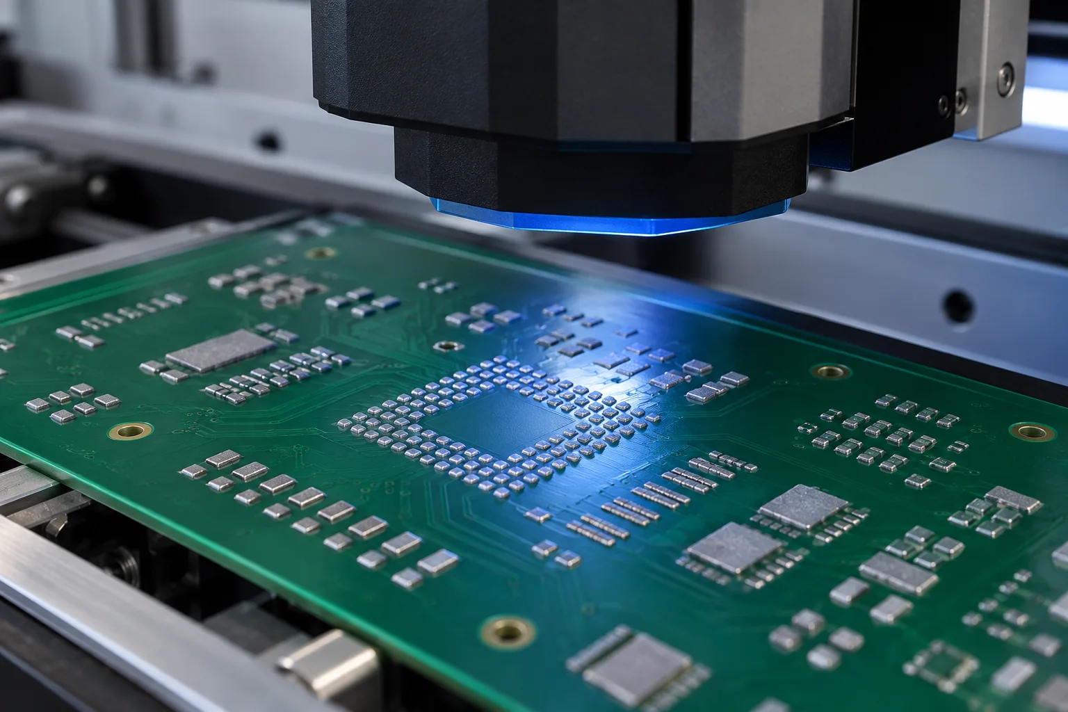
SPI measures the geometry and location of a paste deposit relative to a programmed board reference. In a 3D system, the inspection reconstructs the deposit surface and derives height, area and volume; it also evaluates position and shape according to the recipe. GÖPEL lists shape, height, area, bridges, volume, X/Y offset and coplanarity among common solder-paste inspection criteria. The useful result is not a single green number—it is a comparison between the deposit required for that pad group and what was actually printed.
Read the measurements together. A broad, shallow deposit may cover area while missing volume. A tall deposit can still have the wrong footprint or be shifted away from the termination. A volume result close to target can hide a bridge or bad shape at a fine-pitch location. Group pads by their physical purpose: small BGA lands, QFN perimeter terminals, QFN thermal pads, chip components and large connector pads should not inherit the same limit merely because they share a panel.
| SPI can answer | SPI cannot answer by itself | Method for the later question |
|---|---|---|
| Was the programmed paste deposit present, located and within its measured geometry limits? | Did the component mount with correct polarity and position? | Placement verification or post-reflow AOI, as defined for the visible feature. |
| Did a print show low volume, excess paste, an offset, bridge or repeatable trend? | Did every solder joint reflow into an acceptable visible fillet? | Post-reflow AOI or visual workmanship inspection for accessible joints. |
| Was paste printed over a BGA or QFN land before placement? | Is the hidden joint beneath the package connected or free of voids? | Defined X-ray, electrical test or product-level validation, depending on the question. |
| Is the print process drifting for a defined pad group? | Does the assembled product meet its electrical or functional requirement? | ICT, flying probe or functional test with the required coverage and conditions. |
What defects can SPI find before reflow?
SPI is most useful for print-stage defects that can be corrected before parts make the board harder to recover. A properly configured recipe can expose a missing deposit, insufficient or excessive paste, a shifted print, a bridge, slumping or an abnormal shape. IPC-7093A describes SPI as an early check for bottom-termination components and calls for monitoring of both perimeter and thermal-pad deposits. That early timing matters: a print error can be wiped, adjusted and reprinted before it becomes a hidden post-reflow joint.
The alarm only becomes useful when the response is defined. For a recurring low-volume result, inspect aperture blockage, foil release, paste condition, board support, squeegee condition, print alignment and the programmed region of interest. For an offset, check fiducials, tooling, board registration and the printer setup. Do not treat every alarm as a component-placement problem; SPI happens before placement, so the first diagnosis belongs to the stencil-print route.

Why can SPI not prove a finished BGA or QFN joint?
Because SPI sees paste before the component is placed and before reflow changes the joint. A good deposit is a useful input, but the finished connection also depends on component condition, placement, reflow profile, pad design, surface finish and the package’s hidden geometry. SPI cannot see a BGA ball collapse, a QFN underside joint, an internal void, a lifted termination or the electrical continuity of the final assembly.
Use the method that matches the question. Post-reflow AOI can assess defined visible features such as component presence, orientation markers and accessible solder fillets. X-ray can reveal selected hidden-joint conditions under opaque packages but does not prove all electrical behaviour. ICT or flying probe can exercise defined nets; functional test exercises defined product behaviour. These methods complement one another rather than forming a ladder where a “pass” at SPI proves every later stage.
How should an SPI recipe and response plan be written?
Build the recipe around real pad groups and make every limit actionable. Identify the board and stencil revision, paste side, component or pad group, measurements used, programmed target, warning and action thresholds, sampling or unit scope, and the disposition when a result is outside the agreed window. If the QFN thermal pad is intentionally segmented, the recipe should evaluate that intended pattern rather than comparing it with a generic large-pad deposit.
Illustrative SPI requirement: “For assembly revision [value], inspect the released top-paste layer before placement. Evaluate BGA pads [group], QFN perimeter pads [group] and QFN thermal-pad segments [group] against their approved recipe targets for presence, area, height, volume, position and bridge/shape conditions. A result outside [project limit] triggers print-route review before placement; it is not recorded as a completed solder-joint inspection.”
Replace the brackets with actual product requirements. The wording makes the boundary clear: it uses SPI to control paste printing and does not pretend that a paste result proves a later electrical or reliability outcome.

Five mistakes that turn SPI into a false quality claim
- Calling SPI a solder-joint test: it measures paste before placement and reflow, not the finished connection.
- Using one volume limit everywhere: BGA balls, QFN thermal pads and chip pads have different intended deposits.
- Ignoring position and shape: a near-target volume can still be shifted, bridged or poorly formed.
- Sending all SPI alarms to reflow troubleshooting: start with the stencil-print variables that exist before placement.
- Dropping later inspection because SPI passed: use AOI, X-ray or electrical/functional tests for the risks SPI cannot see.
Read the PCB assembly testing page and the BGA X-ray guide for the next stages of the inspection route. A useful SPI plan states what it measures, what it triggers and what method will answer the questions left after reflow.
About the author
PCBArise Electronics
PCBArise Electronics publishes this guide to help design and NPI teams prepare clearer manufacturing files. The requirements for any actual build are confirmed from its current design package.
FAQ
Common questions
What does SPI measure in PCB assembly?+
SPI measures solder-paste deposits before component placement. A 3D recipe can compare deposit presence, height, area, volume, position and shape with programmed targets. It is a print-process measurement, not a final solder-joint or product-function test.
Can solder paste inspection detect a BGA defect?+
SPI can detect an abnormal paste deposit on a BGA land before placement, such as missing, low, excessive or shifted paste. It cannot see whether the hidden BGA balls formed acceptable joints after reflow. Use a defined X-ray or electrical test when that later question matters.
Does SPI verify component polarity?+
No. SPI runs before components are placed, so it cannot verify component polarity, value, orientation or placement. Use placement verification or post-reflow AOI for defined visible orientation checks, then use electrical or functional testing for the required circuit behaviour.
Why are SPI volume and height both useful?+
They describe different parts of deposit geometry. A deposit can look broad but have insufficient volume, or be tall but have the wrong footprint or offset. Read volume, height, area, position and shape together for the relevant pad group instead of treating one metric as a complete pass/fail result.
What should happen after an SPI alarm?+
Hold the affected print before placement when the agreed action threshold is exceeded, then inspect the print route: stencil condition and apertures, paste, squeegee, alignment, board support and the inspection recipe. Record the cause and correction against the board and stencil revision; do not label it a reflow defect before reflow has occurred.
Technical references
Sources used for this guide
These sources explain the standards, materials or process details discussed above. Check the current revision when applying them to a new design.